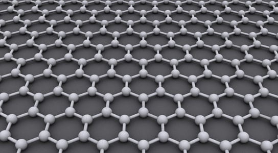
Graphene has garnered significant attention and is globally sought after for its potential applications in areas such as optoelectronics and nanophotonics. Credit: AlexanderAlUS
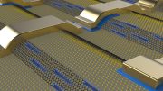
New research from the Canadian Light Source gives further insight into graphene-based devices like foldable tablets, wrap-around TVs, and the next generation of electronics.
Saskatoon – Imagine a tablet device as thin as a piece of paper, folded conveniently in your pocket. Or a 3D TV that wraps around the walls of an entire room in your home. With applications that are nothing short of science fiction, it is no wonder that graphene-based research continues to fascinate scientists.
Graphene is a single-layer sheet of carbon atoms arranged in a honeycomb lattice that is incredibly strong (about 100 times stronger than steel), low weight, and conducts heat and electricity with great efficiency. Graphene was first made in 2004 by Andre Geim and Kostya Novoselov at the University of Manchester – a discovery that earned the two physicists a Nobel Prize in 2010.
Using a number of experimental facilities at the Canadian Light Source, a group of scientists successfully measured the smallest optical density of single-layer graphene so far, giving further insight into the design and fabrication of graphene-based nanodevices, which can potentially enable the future electronic gadgets.
“Nanomaterials, in general, are extremely interesting,” said Dr. Swathi Iyer, a postdoctoral fellow at the CLS. “Graphene has drawn great attention and there is global interest in exploring its use in various applications, including optoelectronic and nanophotonics. The idea of flexible electronic devices has always fascinated me. Graphene would be ideal for such futuristic devices.”
According to Iyer, it was critical to understand the intrinsic property of the graphene, especially where the material folds or cracks.
Iyer and her colleagues wanted to understand the changes at the extremely tiny micro and nanoscale, so they used state-of-the-art techniques to study the structural and electronic properties of freestanding graphene.
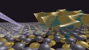
The group fabricated a large-area, freestanding, single-layer graphene-gold hybrid structure using the micro fabrication facility at the CLS. Gold-decorated, single-layer graphene was created and extensively tested, which provided important insights into the electronic activity of this novel hybrid nanostructure.
Using the synchrotron, they identified two distinct activities in the graphene-gold nanostructure: experimental evidence for the localized graphene–gold interaction at the nanoscale, and the smallest optical density for the single layer graphene measured thus far were experimentally confirmed for the first time.
“We believe that our findings on these hybrid nanostructures can pave the way for future fabrication of graphene-based devices with unique configurations, and enhanced properties for a wide range of applications,” said Iyer.
Reference: “Large-Area, Freestanding, Single-Layer Graphene–Gold: A Hybrid Plasmonic Nanostructure” by Ganjigunte R. Swathi Iyer, Jian Wang, Garth Wells, Srinivasan Guruvenket, Scott Payne, Michael Bradley and Ferenc Borondics, 26 May 2014, ACS Nano.
DOI: 10.1021/nn501864h


Be the first to comment on "New Research Gives Further Insight Into Graphene-Based Electronics"