Over the course of almost 60 years, the information age has given the world the internet, smart phones, and lightning-fast computers. This has been made possible by about doubling the number of transistors that can be packed onto a computer chip every two years, resulting in billions of atomic-scale transistors that can fit on a fingernail-sized device. Even individual atoms may be observed and counted within such “atomic scale” lengths.
Physical limit
With this doubling reaching its physical limit, the U.S. Department of Energy’s (DOE) Princeton Plasma Physics Laboratory (PPPL) has joined industry efforts to prolong the process and find new techniques to make ever-more powerful, efficient, and cost-effective chips. In the first PPPL research conducted under a Cooperative Research and Development Agreement (CRADA) with Lam Research Corp., a global producer of chip-making equipment, laboratory scientists properly predicted a fundamental phase in atomic-scale chip production through the use of modeling.
“This would be one little piece in the whole process,” said David Graves, associate laboratory director for low-temperature plasma surface interactions, a professor in the Princeton Department of Chemical and Biological Engineering and co-author of a paper that outlines the findings in the Journal of Vacuum Science & Technology B. Insights gained through modeling, he said, “can lead to all sorts of good things, and that’s why this effort at the Lab has got some promise.”
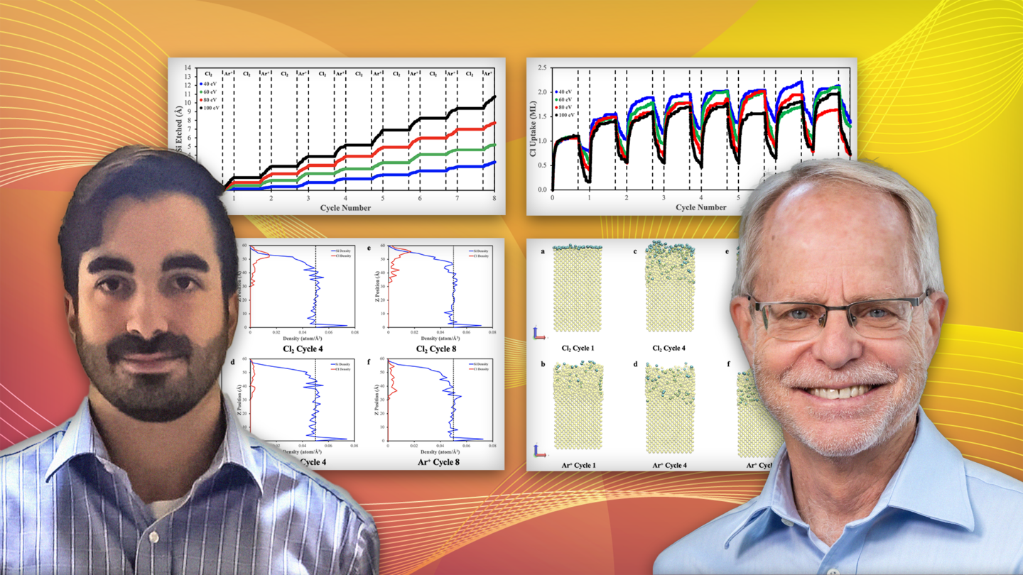
Physicist Joseph Vella, left, and David Graves with figures from their paper. Credit: Ben Marshall for photo of Vella; Graves photo courtesy of Princeton University Department of Chemical and Biological Engineering. Collage by Kiran Sudarsanan
While the shrinkage can’t go on much longer, “it hasn’t completely reached an end,” he said. “Industry has been successful to date in using mainly empirical methods to develop innovative new processes but a deeper fundamental understanding will speed this process. Fundamental studies take time and require expertise industry does not always have,” he said. “This creates a strong incentive for laboratories to take on the work.”
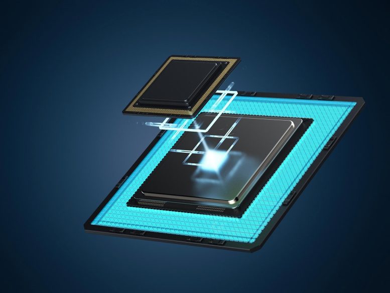
The PPPL scientists modeled what is called “atomic layer etching” (ALE), an increasingly critical fabrication step that aims to remove single atomic layers from a surface at a time. This process can be used to etch complex three-dimensional structures with critical dimensions that are thousands of times thinner than a human hair into a film on a silicon wafer.
Basic agreement
“The simulations basically agreed with experiments as a first step and could lead to improved understanding of the use of ALE for atomic-scale etching,” said Joseph Vella, a post-doctoral fellow at PPPL and lead author of the journal paper. Improved understanding will enable PPPL to investigate such things as the extent of surface damage and the degree of roughness developed during ALE, he said, “and this all starts with building our fundamental understanding of atomic layer etching.”
The model simulated the sequential use of chlorine gas and argon plasma ions to control the silicon etch process on an atomic scale. Plasma, or ionized gas, is a mixture consisting of free electrons, positively charged ions and neutral molecules. The plasma used in semiconductor device processing is near room temperature, in contrast to the ultra-hot plasma used in fusion experiments.
“A surprise empirical finding from Lam Research was that the ALE process became particularly effective when the ion energies were quite a bit higher than the ones we started with,” Graves said. “So that will be our next step in the simulations — to see if we can understand what’s happening when the ion energy is much higher and why it’s so good.”
Going forward, “the semiconductor industry as a whole is contemplating a major expansion in the materials and the types of devices to be used, and this expansion will also have to be processed with atomic scale precision,” he said. “The U.S. goal is to lead the world in using science to tackle important industrial problems,” he said, “and our work is part of that.”
Reference: “Molecular dynamics study of silicon atomic layer etching by chorine gas and argon ions” by Joseph R. Vella, David Humbird and David B. Graves, 10 February 2022, Journal of Vacuum Science & Technology B.
DOI: 10.1116/6.0001681
This study was partially supported by the DOE Office of Science. Coauthors included David Humbird of DWH Consulting in Centennial, Colorado.
PPPL, on Princeton University’s Forrestal Campus in Plainsboro, N.J., is devoted to creating new knowledge about the physics of plasmas — ultra-hot, charged gases — and to developing practical solutions for the creation of fusion energy.


Be the first to comment on "Atomic Layer Etching Could Lead to Ever-More Powerful Microchips and Supercomputers"