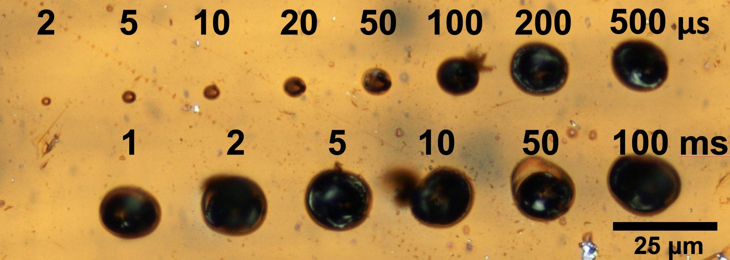
Scientists recorded the formation of laser-induced graphene made with a small laser mounted to a scanning electron microscope. Credit: Tour Group/Rice University
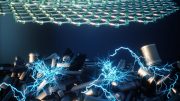
You don’t need a big laser to make laser-induced graphene (LIG). Scientists at Rice University, the University of Tennessee, Knoxville (UT Knoxville) and Oak Ridge National Laboratory (ORNL) are using a very small visible beam to burn the foamy form of carbon into microscopic patterns.
The labs of Rice chemist James Tour, which discovered the original method to turn a common polymer into graphene in 2014, and Tennessee/ORNL materials scientist Philip Rack revealed they can now watch the conductive material form as it makes small traces of LIG in a scanning electron microscope (SEM).
The altered process, detailed in the American Chemical Society’s ACS Applied Materials & Interfaces, creates LIG with features more than 60% smaller than the macro version and almost 10 times smaller than typically achieved with the former infrared laser.
Lower-powered lasers also make the process less expensive, Tour said. That could lead to wider commercial production of flexible electronics and sensors.
“A key for electronics applications is to make smaller structures so that one could have a higher density, or more devices per unit area,” Tour said. “This method allows us to make structures that are 10 times denser than we formerly made.”
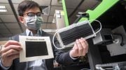
To prove the concept, the lab made flexible humidity sensors that are invisible to the naked eye and directly fabricated on polyimide, a commercial polymer. The devices were able to sense human breath with a response time of 250 milliseconds.
“This is much faster than the sampling rate for most commercial humidity sensors and enables the monitoring of rapid local humidity changes that can be caused by breathing,” said the paper’s lead author, Rice postdoctoral researcher Michael Stanford.
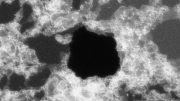
Scientists at Rice University and Oak Ridge National Laboratory used a small laser mounted to a scanning electron microscope to form dots and traces of conductive graphene on a polymer. The technique creates laser-induced graphene with features more than 60% smaller than the macro version and almost 10 times smaller than typically achieved with an infrared laser. Credit: Tour Group/Rice University
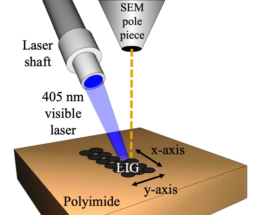
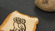
The smaller lasers pump light at a wavelength of 405 nanometers, in the blue-violet part of the spectrum. These are less powerful than the industrial lasers the Tour Group and others around the world are using to burn graphene into plastic, paper, wood, and even food.
The SEM-mounted laser burns only the top five microns of the polymer, writing graphene features as small as 12 microns. (A human hair, by comparison, is 30 to 100 microns wide.)
Working directly with ORNL let Stanford capitalize on the national lab’s advanced equipment. “That’s what made this joint effort possible,” Tour said.
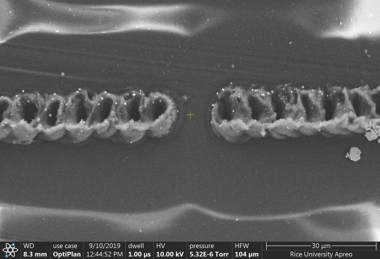
A scanning electron microscope image shows two traces of laser-induced graphene on a polyimide film. A laser mounted to the microscope was used to burn the patterns into the film. The technique shows promise for the development of flexible electronics. Credit: Tour Group/Rice University
“I did a lot of my Ph.D. research at ORNL, so I was aware of the excellent facilities and scientists and how they could help us with our project,” Stanford said. “The LIG features we were creating were so small that they would have been next to impossible to find if we were to lase the patterns and then search for them in the microscope later.”
Tour, whose group recently introduced flash graphene to instantly turn trash and food waste into the valuable material, said the new LIG process offers a new path toward writing electronic circuits into flexible substrates like clothing.
“While the flash process will produce tons of graphene, the LIG process will allow graphene to be directly synthesized for precise electronics applications on surfaces,” Tour said.
Reference: “High-Resolution Laser-Induced Graphene. Flexible Electronics Beyond the Visible Limit” by Michael G. Stanford, Cheng Zhang, Jason Davidson Fowlkes, Anna Hoffman, Ilia N. Ivanov, Philip D. Rack and James M. Tour, 10 February 2020, ACS Applied Materials & Interfaces.
DOI: 10.1021/acsami.0c01377
Co-authors of the paper are postdoctoral researcher Cheng Zhang and graduate student Anna Hoffman of UT Knoxville, research and development scientist Ilia Ivanov of Oak Ridge National Laboratory, and staff scientist Jason Davidson Fowlkes of UT Knoxville and Oak Ridge.
Tour is the T.T. and W.F. Chao Chair in Chemistry as well as a professor of computer science and of materials science and nanoengineering at Rice. Rack is a professor and the Leonard G. Penland Chair and associate department head of materials science and engineering at UT Knoxville, as well as joint staff at the Center for Nanophase Materials Sciences at Oak Ridge.
The Air Force Office of Scientific Research and the U.S. Department of Energy supported the research.
These are less powerful than the industrial lasers the Tour Group and others around the world are using to burn graphene into plastic, paper, wood, and even food. Tour, whose group recently introduced flash graphene to instantly turn trash and food waste into the valuable material. yes, it’s very useful for us. many peoples take benefits from it.