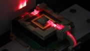
Scientists have used a microchip to map the back of the eye for disease diagnosis. The interference technology used in the microchip has been around for a little while. This is the first time technical obstacles have been overcome to fabricate a miniature device able to capture high-quality images. Credit: Columbia University
High-quality medical images produced using a microchip prove researcher’s fabrication method can be used to miniaturize sensing, imaging, and optical communication systems.
Scientists in Christine Hendon’s and Michal Lipson’s research groups at Columbia University, New York, have used a microchip to map the back of the eye for disease diagnosis.
The interference technology, like bat sonar but using light instead of sound waves, used in the microchip has been around for a little while. This is the first time that technical obstacles have been overcome to fabricate a miniature device able to capture high-quality images.
Ophthalmologists’ current optical coherence tomography (OCT) devices and surveyors’ light detection and ranging (LIDAR) machines are bulky and expensive. There is a push for miniaturization in order to produce cheap handheld OCT and LIDAR small enough to fit into self-driving cars.
In AIP Photonics, by AIP Publishing, the team demonstrates their microchip’s ability to produce high-contrast OCT images 0.6 millimeters deeper in human tissue.
“Previously, we’ve been limited, but using the technique we developed in this project, we’re able to say we can make any size system on a chip,” said co-author Aseema Mohanty. “That’s a big deal!”
Author Xingchen Ji is similarly excited and hopes the work receives industry funding to develop a small, fully integrated handheld OCT device for affordable deployment outside of a hospital in low-resource settings. Clearly seeing the advantages of miniaturization in interference technologies, both the National Institute of Health and the U.S. Air Force funded Ji’s project.
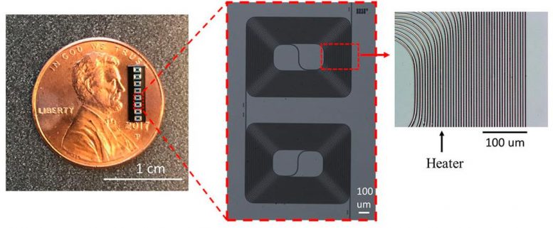
Central to the chip-scale interferometer is the fabrication of the tunable delay line. A delay line calculates how light waves interact, and by tuning to different optical paths, which are like different focal lengths on a camera, it collates the interference pattern to produce a high-contrast 3D image.
Ji and Mohanty coiled a 0.4-meter Si3N4 delay line into a compact 8mm2 area and integrated the microchip with micro-heaters to optically tune the heat-sensitive Si3N4.
“By using the heaters, we achieve delay without any moving parts, so providing high stability, which is important for the image quality of interference-based applications,” said Ji.
But with components tightly bent in a small space, it’s hard to avoid losses when changing the physical size of the optical path. Ji previously optimized fabrication to prevent optical loss. He applied this method alongside a new tapered region to accurately stitch lithographic patterns together – an essential step for achieving large systems. The team demonstrated the tunable delay line microchip on an existing commercial OCT system, showing that deeper depths could be probed while maintaining high-resolution images.
This technique should be applicable to all interference devices, and Mohanty and Ji are already starting to scale LIDAR systems, one of the biggest photonic interferometry systems.
###
Reference: “On-chip Tunable Photonic Delay Line,” is authored by Xingchen Ji, Xinwen Yao, Yu Gan, Aseema Mohanty, Mohammad A. Tadayon, Christine P. Hendon and Michal Lipson, 17 September 2019, APL Photonics.
DOI: 10.1063/1.5111164


Be the first to comment on "Miniaturizing Medical Imaging, Sensing Technology Is a “Big Deal”"