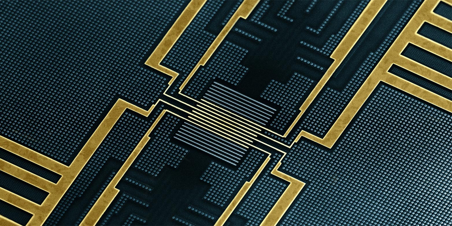
The chip produced by IMEC for the experiments at ETH. The tunnel junctions used to measure the timing of the magnetization reversal are located at the center. Credit: IMEC
Researchers at ETH have measured the timing of single writing events in a novel magnetic memory device with a resolution of less than 100 picoseconds. Their results are relevant for the next generation of main memories based on magnetism.
At the Department for Materials of the ETH in Zurich, Pietro Gambardella and his collaborators investigate tomorrow’s memory devices. They should be fast, retain data reliably for a long time and also be cheap. So-called magnetic “random access memories” (MRAM) achieve this quadrature of the circle by combining fast switching via electric currents with durable data storage in magnetic materials. A few years ago researchers could already show that a certain physical effect – the spin-orbit torque – makes particularly fast data storage possible. Now Gambardella’s group, together with the R&D-center IMEC in Belgium, managed to temporally resolve the exact dynamics of a single such storage event – and to use a few tricks to make it even faster.
Magnetizing with single spins
To store data magnetically, one has to invert the direction of magnetization of a ferromagnetic (that is, permanently magnetic) material in order to represent the information as a logic value, 0 or 1. In older technologies, such as magnetic tapes or hard drives, this is achieved through magnetic fields produced inside current-carrying coils. Modern MRAM-memories, by contrast, directly use the spins of electrons, which are magnetic, much like small compass needles, and flow directly through a magnetic layer as an electric current. In Gambardella’s experiments, electrons with opposite spin directions are spatially separated by the spin-orbit interaction. This, in turn, creates an effective magnetic field, which can be used to invert the direction of magnetization of a tiny metal dot.

Electron microscope image of the magnetic tunnel junction (MTJ, at the center) and of the electrodes for controlling and measuring the reversal process. Credit: P. Gambardella / ETH Zürich
“We know from earlier experiments, in which we stroboscopically scanned a single magnetic metal dot with X-rays, that the magnetization reversal happens very fast, in about a nanosecond,” says Eva Grimaldi, a post-doc in Gambardella’s group. “However, those were mean values averaged over many reversal events. Now we wanted to know how exactly a single such event takes place and to show that it can work on an industry-compatible magnetic memory device.”
Time resolution through a tunnel junction
To do so, the researchers replaced the isolated metal dot with a magnetic tunnel junction. Such a tunnel junction contains two magnetic layers separated by an insulation layer that is only one nanometer thick. Depending on the spin direction – along the magnetization of the magnetic layers, or opposite to it – the electrons can tunnel through that insulating layer more or less easily. This results in an electrical resistance that depends on the alignment of the magnetization in one layer with respect to the other and thus represents “0” and “1”. From the time dependence of that resistance during a reversal event, the researchers could reconstruct the exact dynamics of the process. In particular, they found that the magnetization reversal happens in two stages: an incubation stage, during which the magnetization stays constant, and the actual reversal stage, which lasts less than a nanosecond.
Small fluctuations
“For a fast and reliable memory device it is essential that the time fluctuations between the individual reversal events are minimized,” explains Gambardella’s Ph.D. student Viola Krizakova. So, based on their data the scientists developed a strategy to make those fluctuations as small as possible. To that end, they changed the current pulses used to control the magnetization reversal in such a way as to introduce two additional physical phenomena. The so-called spin-transfer torque as well as a short voltage pulse during the reversal stage now resulted in a reduction of the total time for the reversal event to less than 0.3 nanoseconds, with temporal fluctuations of less than 0.2 nanoseconds.
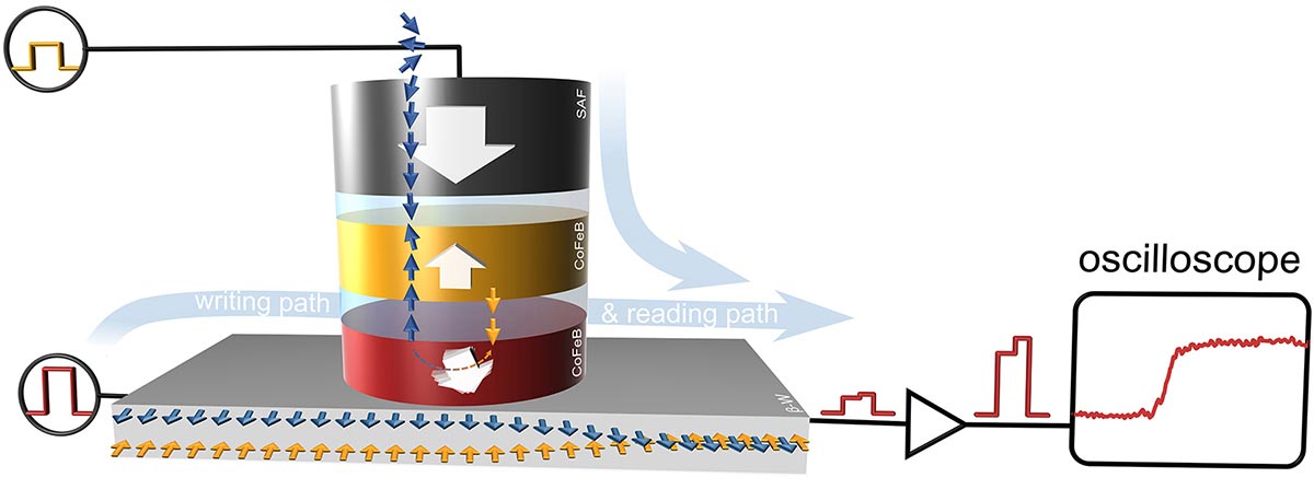
The magnetic tunnel junction (yellow and red disks) in which the magnetization of the red disk is inverted by electron spins (blue and yellow arrows). The reversal process is measured through the tunnel resistance (vertical blue arrows). Credit: ETH Zürich
Application-ready technology
“Putting all of this together, we have found a method whereby data can be stored in magnetic tunnel junctions virtually without any error and in less than a nanosecond,” says Gambardella. Moreover, the collaboration with the research center IMEC made it possible to test the new technology directly on an industry-compatible wafer. Kevin Garello, a former post-doc from Gambardella’s lab, produced the chips containing the tunnel contacts for the experiments at ETH and optimized the materials for them. In principle, the technology would, therefore, be immediately ready for use in a new generation of MRAM.
Gambardella stresses that MRAM memories are particularly interesting because, differently from conventional main memories such as SRAM or DRAM, they don’t lose their information when the computer is switched off, but are still equally fast. He concedes, though, that the market for MRAM memories currently does not demand such high writing speeds since other technical bottlenecks such as power losses caused by large switching currents limit the access times. In the meantime, he and his co-workers are already planning further improvements: they want to shrink the tunnel junctions and use different materials that use current more efficiently.
Reference: “Single-shot dynamics of spin–orbit torque and spin transfer torque switching in three-terminal magnetic tunnel junctions” by Eva Grimaldi, Viola Krizakova, Giacomo Sala, Farrukh Yasin, Sébastien Couet, Gouri Sankar Kar, Kevin Garello and Pietro Gambardella, 27 January 2020, Nature Nanotechnology.
DOI: 10.1038/s41565-019-0607-7


Be the first to comment on "Next Generation Magnetic Memory Breakthrough: Writing Data in Under a Nanosecond"