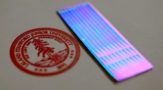
This photo shows an array of 1-mm-wide by 2-cm-long single-crystal organic semiconductors. The neatly aligned blue strips are what provide greater electric charge mobility. The Stanford logo shown here is the same size as a dime. Credit: Y. Diao, B. C-K. Tee, et al.
Using a new printing process called FLUENCE (fluid-enhanced crystal engineering), researchers have developed highly aligned single-crystalline organic semiconductor thin films that are capable of conducting electricity 10 times more efficiently than those created using conventional methods.
Through innovations to a printing process, researchers have made major improvements to organic electronics—a technology in demand for lightweight, low-cost solar cells, flexible electronic displays, and tiny sensors. The printing method is fast and works with a variety of organic materials to produce semiconductors of strikingly higher quality than what has so far been achieved with similar methods.
Organic electronics have great promise for a variety of applications, but even the highest quality films available today fall short in how well they conduct electrical current. The team from the U.S. Department of Energy’s (DOE) SLAC National Accelerator Laboratory and Stanford University have developed a printing process they call FLUENCE—fluid-enhanced crystal engineering—that for some materials results in thin films capable of conducting electricity 10 times more efficiently than those created using conventional methods.
“Even better, most of the concepts behind FLUENCE can scale up to meet industry requirements,” said Ying Diao, a SLAC/Stanford postdoctoral researcher and lead author of the study, which was published on June 2 in Nature Materials.
Stefan Mannsfeld, a SLAC materials physicist and one of the principal investigators of the experiment, said the key was to focus on the physics of the printing process rather than the chemical makeup of the semiconductor. Diao engineered the process to produce strips of big, neatly aligned crystals that electrical charge can flow through easily, while preserving the benefits of the “strained lattice” structure and “solution shearing” printing technique previously developed in the lab of Mannsfeld’s co-principal investigator, Professor Zhenan Bao of the Stanford Institute for Materials and Energy Sciences, a joint SLAC-Stanford institute.
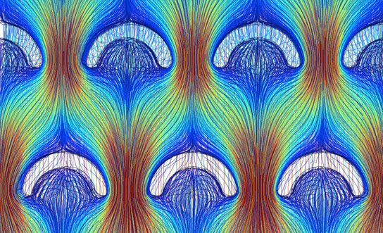
This image shows a simulation, called a “streamline representation,” of the organic semiconductor solution flowing around the micropillars and mixing in the spaces below. The colors indicate different speeds for the solution as it passes the micropillars and gets mixed behind them: deep blue is 0 mm/s, all the way up to red for 1.3 mm/s. Credit: Y. Diao et al.
To make the advance, Diao focused on controlling the flow of the liquid in which the organic material is dissolved. “It’s a vital piece of the puzzle,” she said. If the ink flow does not distribute evenly, as is often the case during fast printing, the semiconducting crystals will be riddled with defects. “But in this field there’s been little research done on controlling fluid flow.”
Diao designed a printing blade with tiny pillars embedded in it that mix the ink so it forms a uniform film. She also engineered a way around another problem: the tendency of crystals to randomly form across the substrate. A series of cleverly designed chemical patterns on the substrate suppress the formation of unruly crystals that would otherwise grow out of alignment with the printing direction. The result is a film of large, well-aligned crystals.
X-ray studies of the group’s organic semiconductors at the Stanford Synchrotron Radiation Lightsource (SSRL) allowed them to inspect their progress and continue to make improvements, eventually showing neatly arranged crystals at least 10 times longer than crystals created with other solution-based techniques, and of much greater structural perfection.
The group also repeated the experiment using a second organic semiconductor material with a significantly different molecular structure, and again they saw a notable improvement in the quality of the film. They believe this is a sign the techniques will work across a variety of materials.
Principal investigators Bao and Mannsfeld say the next step for the group is pinning down the underlying relationship between the material and the process that enabled such a stellar result. Such a discovery could provide an unprecedented degree of control over the electronic properties of printed films, optimizing them for the devices that will use them.
“That could lead to a revolutionary advance in organic electronics,” Bao said. “We’ve been making excellent progress, but I think we’re only just scratching the surface.”
Other study co-authors included researchers from Stanford University’s departments of chemistry and chemical and electrical engineering and Nanjing University. The research was supported by SLAC’s Laboratory Directed Research and Development program. SSRL is a national user facility operated by Stanford University on behalf of the DOE’s Office of Science.
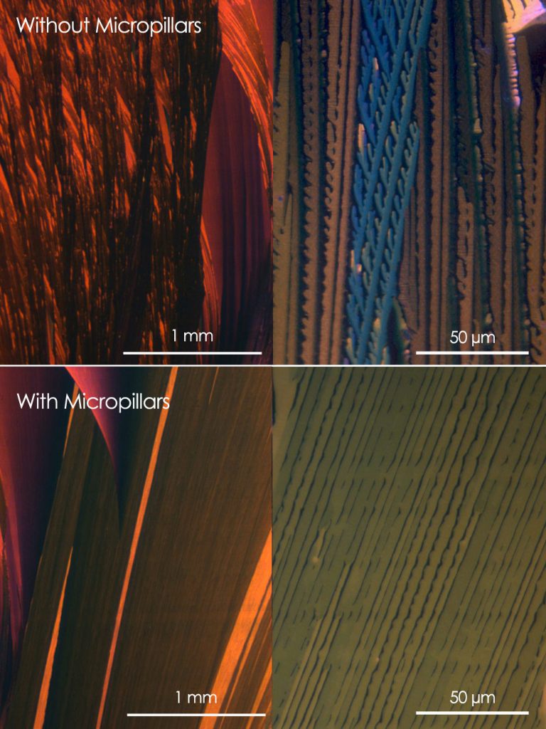
Cross-polarized optical micrograph comparing a sample of an organic semiconducting film created without micropillars (top) and with micropillars (bottom) at scales of both one millimeter and 50 micrometers. Note the uniformity of the crystals in the bottom image as compared to the images in the top. Credit: Y. Diao et al.
SLAC is a multi-program laboratory exploring frontier questions in photon science, astrophysics, particle physics, and accelerator research. Located in Menlo Park, California, SLAC is operated by Stanford University for the U.S. Department of Energy Office of Science. To learn more, please visit www.slac.stanford.edu.
DOE’s Office of Science is the single largest supporter of basic research in the physical sciences in the United States, and is working to address some of the most pressing challenges of our time. For more information, please visit science.energy.gov.
Reference: “Solution coating of large-area organic semiconductor thin films with aligned single-crystalline domains” by Ying Diao, Benjamin C-K. Tee, Gaurav Giri, Jie Xu, Do Hwan Kim, Hector A. Becerril, Randall M. Stoltenberg, Tae Hoon Lee, Gi Xue, Stefan C. B. Mannsfeld and Zhenan Bao, 2 June 2013, Nature Materials.
DOI: 10.1038/nmat3650


It is heartening to see that my theories on the structure and creation of our universe are being applied in such a useful way.
Now that we understand our universe in a way never previously imagined, we humans will be now able to manipulate Protons and Neutron in a much much more manageable way than was previously thought possible.
It’s just a great pity, and an insult to my intellect that I have not yet received the credit and recognition I deserve for the years of work I put into the project.
What has our dear Peter O’Connor’s universe got to do with organic printing ? Recognition for any plausible and noteworthy theory will surely be heede4 and dummy arguments can only amuse the scientific community. Thank You.