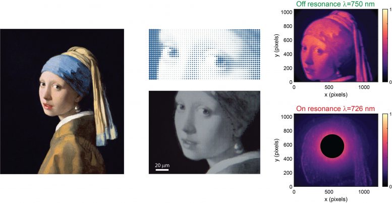
Figure (left) Meisje met de parel (J. Vermeer, circa 1665, collection Mauritshuis, The Hague, the Netherlands); (center) chrome nano-dots replica; (right-top) normal image taken under off-resonant conditions; (right-bottom) edge image taken on resonance. Credit: AMOLF
AMOLF researchers and their collaborators from the Advanced Science Research Center (ASRC/CUNY) in New York have created a nanostructured surface capable of performing on-the-fly mathematical operations on an input image. This discovery could boost the speed of existing imaging processing techniques and lower energy usage. The work enables ultrafast object detection and augmented reality applications. The researchers published their results on November 1st in the journal Nano Letters.
Image processing is at the core of several rapidly growing technologies, such as augmented reality, autonomous driving, and more general object recognition. But how does a computer find and recognize an object? The initial step is to understand where its boundaries are, hence edge detection in an image becomes the starting point for image recognition. Edge detection is typically performed digitally using integrated electronic circuits implying fundamental speed limitations and high energy consumption, or in an analog fashion which requires bulky optics.

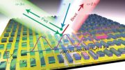
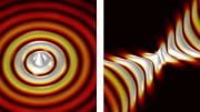
Figure (left) Schematic of edge detection and spatial differentiation; (right) derivative image of AMOLF logo taken at a wavelength of 726 nm. Credit: AMOLF
Nanostructured metasurface
In a completely new approach, AMOLF Ph.D. student Andrea Cordaro and his co-workers created a special “metasurface,” a transparent substrate with a specially designed array of silicon nanobars. When an image is projected onto the metasurface, the transmitted light forms a new image that shows the edges of the original. Effectively, the metasurface performs a mathematical derivative operation on the image, which provides a direct probe of edges in the image. In the first experiment, an image of the AMOLF logo was projected onto the metasurface. At a specially designed wavelength (726 nm), a clear image of the edges is observed. The mathematical transformation results from the fact that each spatial frequency that composes the image has a tailored transmission coefficient through the metasurface. This tailored transmission is the result of a complex interference of light as it propagates through the metasurface.
Edge detection
To demonstrate edge detection experimentally on an image the researchers created a miniature version of the painting Meisje met de parel (J. Vermeer) by printing tiny chromium dots onto a transparent substrate. If the image is projected onto the metasurface using off-resonant illumination (λ=750 nm) the original image is clearly recognized. In contrast, if the illumination has the right color (λ=726 nm) the edges are clearly resolved in the transformed image.
This new optical computing and imaging technique operates at the speed of light and the mathematical operation itself consumes no energy as it involves only passive optical components. The metasurface can be readily implemented by placing it directly onto a standard CCD or CMOS detector chip, opening new opportunities in hybrid optical and electronic computing that operates at low cost, low power, and small dimensions.
Reference: “High-index dielectric metasurfaces performing mathematical operations” by A. Cordaro, H. Kwon, D. Sounas, A.F. Koenderink, A. Alu and A. Polman, 1 November 2019, Nano Letters.
DOI: 10.1021/acs.nanolett.9b02477


Be the first to comment on "Speed of Light Mathematics With Nanostructured Metasurface"