Pacific Northwest National Laboratory scientists have uncovered new properties in a semiconductor material using a powerful, unconventional technique. Credit: Quardia, Shutterstock.com
Discovery reveals the role of oxygen impurities in semiconductor properties
A team of researchers investigating the properties of a semiconductor combined with a new thin oxide sheet discovered an unexpected new source of conductivity from oxygen atoms trapped within.
Scott Chambers, a materials scientist at the Department of Energy’s Pacific Northwest National Laboratory, revealed the team’s findings at the American Physical Society’s Spring 2022 meeting. The study’s findings are detailed in the journal Physical Review Materials.
The finding has far-reaching implications for understanding the function of thin oxide films in future semiconductor design and manufacturing. Specifically, semiconductors utilized in modern electronics are classified into two basic types: n-type and p-type, depending on the electronic impurity introduced during crystal formation. Both n- and p-type silicon-based materials are used in modern electronic devices. However, there is ongoing interest in the development of new types of semiconductors. Chambers and his colleagues were experimenting with germanium in conjunction with a thin crystalline layer of lanthanum-strontium-zirconium-titanium-oxide (LSZTO).
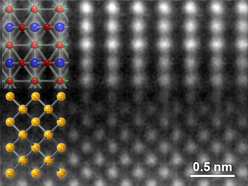
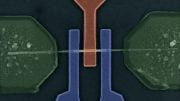
Scanning transmission electron micrograph of the interface between germanium (bottom) and LSZTO (top). The individual atoms are labeled gold: germanium, red: oxygen, green: strontium and lanthanum, blue: titanium and zirconium. Credit: Scott Chambers, Pacific Northwest National Laboratory
“We are reporting on a powerful tool for probing semiconductor structure and function,” said Chambers. “Hard X-ray photoelectron spectroscopy revealed in this case that atoms of oxygen, an impurity in the germanium, dominate the properties of the material system when germanium is joined to a particular oxide material. This was a big surprise.”
Using the Diamond Light Source on the Harwell Science and Innovation Campus in Oxfordshire, England, the research team discovered they could learn a great deal more about the electronic properties of the germanium/LSZTO system than was possible using the typical methods.
“When we tried to probe the material with conventional techniques, the much higher conductivity of germanium essentially caused a short circuit,” Chambers said. “As a result, we could learn something about the electronic properties of the Ge, which we already know a lot about, but nothing about the properties of the LSZTO film or the interface between the LSZTO film and the germanium—which we suspected might be very interesting and possibly useful for technology.”
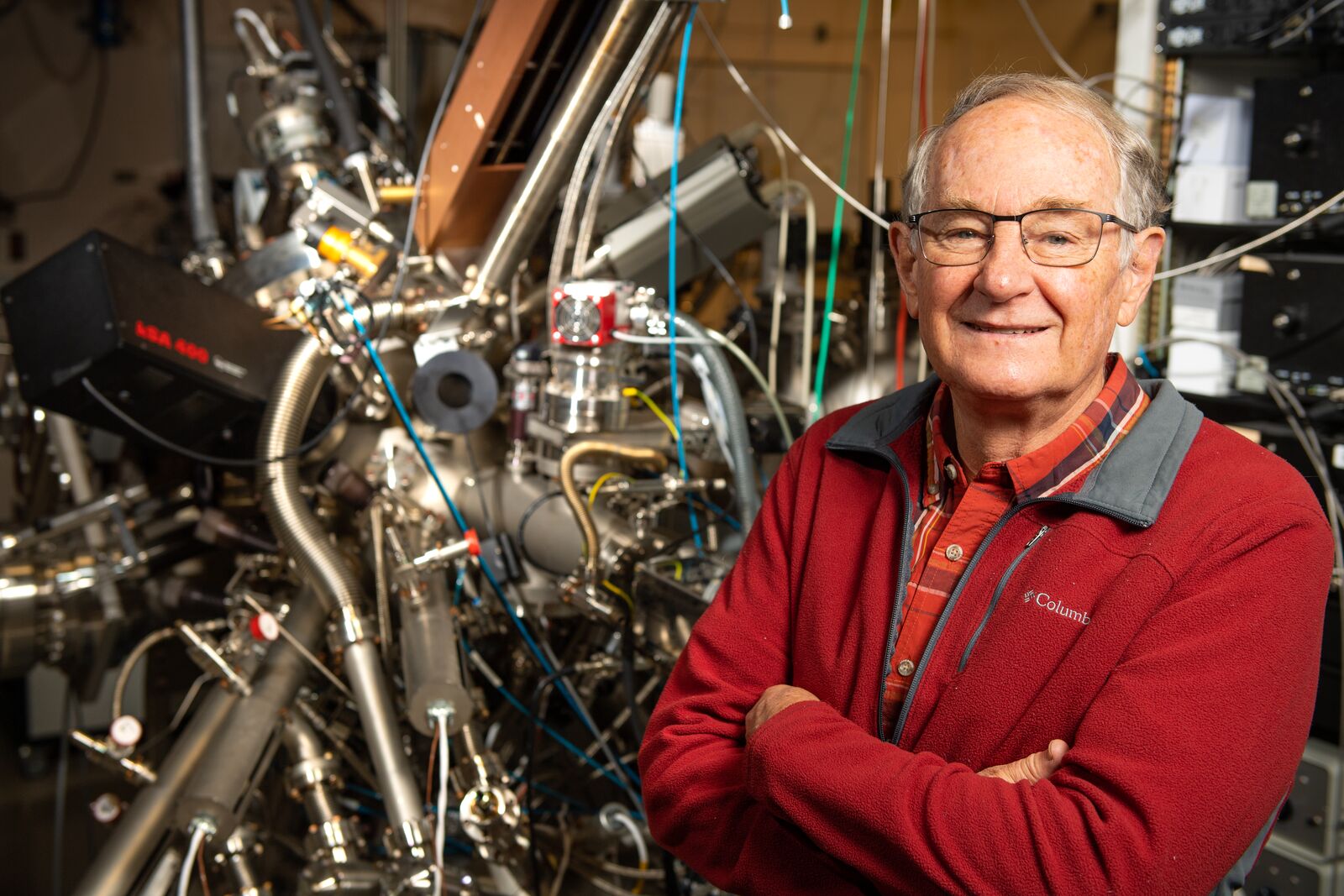
Materials Scientist Scott Chambers and his Pacific Northwest National Laboratory colleagues study the properties of semiconductor materials at atomic-level detail. Credit: Andrea Starr, Pacific Northwest National Laboratory
A new role for hard X-rays
The so-called “hard” X-rays produced by the Diamond Light Source could penetrate the material and generate information about what was going on at the atomic level.
“Our results were best interpreted in terms of oxygen impurities in the germanium being responsible for a very interesting effect,” Chambers said. “The oxygen atoms near the interface donate electrons to the LSZTO film, creating holes, or the absence of electrons, in the germanium within a few atomic layers of the interface. These specialized holes resulted in behavior that totally eclipsed the semiconducting properties of both n- and p-type germanium in the different samples we prepared. This, too, was a big surprise.”
The interface, where the thin-film oxide and the base semiconductor come together, is where interesting semiconducting properties often emerge. The challenge, according to Chambers, is to learn how to control the fascinating and potentially useful electric fields that forms at these interfaces by modifying the electric field at the surface. Ongoing experiments at PNNL are probing this possibility.
While the samples used in this research do not likely have the immediate potential for commercial use, the techniques and scientific discoveries made are expected to pay dividends in the longer term, Chambers said. The new scientific knowledge will help materials scientists and physicists better understand how to design new semiconductor material systems with useful properties.
PNNL researchers Bethany Matthews, Steven Spurgeon, Mark Bowden, Zihua Zhu and Peter Sushko contributed to the research. The study was supported by the Department of Energy Office of Science. Some experiments and sample preparation were performed at the Environmental Molecular Sciences Laboratory, a Department of Energy Office of Science user facility located at PNNL. Electron microscopy was performed in the PNNL Radiochemical Processing Laboratory. Collaborators Tien-Lin Lee and Judith Gabel performed experiments at the Diamond Light Source. Additional collaborators included the University of Texas at Arlington’s Matt Chrysler and Joe Ngai, who prepared the samples.
Reference: “Mapping hidden space-charge distributions across crystalline metal oxide/group IV semiconductor interfaces” by S. A. Chambers, M. Chrysler, J. H. Ngai, T.-L. Lee, J. Gabel, B. E. Matthews, S. R. Spurgeon, M. E. Bowden, Z. Zhu and P. V. Sushko, 21 January 2022, Physical Review Materials.
DOI: 10.1103/PhysRevMaterials.6.015002


Be the first to comment on "Unexpected Semiconductor Properties Revealed by Innovative New Tool"