
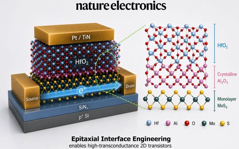
A sub-nanometer buffer improved atomically thin transistors, pushing future chips closer to silicon’s limits.
A transistor channel only one atom thick sounds like an ideal foundation for the next generation of computer chips. But surrounding that channel with the materials needed to control it can erase much of its advantage.
Researchers at National Yang Ming Chiao Tung University (NYCU) and TSMC Corporate Research have now demonstrated a possible way around that problem. Instead of developing another semiconductor, they redesigned the tiny interface where the semiconductor meets its insulating layer.
The result was a monolayer molybdenum disulfide (MoS2) transistor that combined a gate dielectric with an equivalent oxide thickness of about one nanometer (about 0.000000039 inches) and a maximum transconductance of 0.45 mS μm-1. The study was published in Nature Electronics.
The advance addresses a problem that has followed two-dimensional semiconductors for years.
Why MoS2 Could Replace Silicon
Silicon has powered decades of chip development, but it becomes increasingly difficult to control as transistor dimensions approach the atomic scale. Two-dimensional semiconductors offer a possible alternative because their channels can remain extremely thin without losing their basic crystal structure.
MoS2 belongs to a family of layered materials known as transition metal dichalcogenides. A single layer is only about 0.7 nanometers thick, yet it can function as a semiconductor and carry electrical current. TSMC researchers have previously demonstrated monolayer MoS2 in gate-all-around transistors, illustrating its potential for advanced device designs.
However, a transistor needs more than a channel. It also requires a gate electrode that switches the current on and off. Between the gate and channel sits an insulating material called the gate dielectric.
The Gate Dielectric Trade-Off
As transistors shrink, this dielectric must provide stronger electrical control while remaining extremely thin. The difficulty is that depositing an insulator directly onto MoS2 can disrupt the very electrons the gate is supposed to control.
That creates a frustrating trade-off. A thinner dielectric can improve switching, but interactions and defects at the interface can scatter electrons, reduce carrier mobility, and weaken transistor performance.
“For many years, efforts to improve atomically thin transistors have largely focused on discovering better semiconductor materials,” said Professor Wen-Hao Chang, the study’s corresponding author from NYCU. “Our research shows that the atomic interface between materials can be just as important. By engineering that boundary, we were able to reduce one of the fundamental trade-offs that has limited two-dimensional transistors for many years.”
Why Insulators Struggle on MoS2
Growing a uniform insulating film on silicon is supported by decades of manufacturing experience. MoS2 behaves differently.
Its surface lacks dangling bonds, the chemically active sites that normally help deposited materials attach and form a continuous film. As a result, conventional deposition can leave gaps, defects, and areas of electrical disorder.
Researchers have tried to solve the problem with molecular seed layers, different insulating materials, surface treatments, and modified oxide deposition processes. These methods have produced improvements, but it remains difficult to achieve three goals at once: a very small equivalent oxide thickness, precise gate control, and efficient electron transport.
The challenge is especially important for chemical vapor deposition, or CVD, because that method can grow monolayer material across large areas. Laboratory experiments often use small flakes peeled from a larger crystal, but future chip manufacturing will require repeatable films that can cover wafers. Researchers have already demonstrated uniform MoS2 growth on wafers as large as 12 inches, although turning such material into reliable commercial electronics remains a much broader challenge.
An Atomic-Scale Aluminum Oxide Buffer
The NYCU team approached the problem by placing an epitaxial aluminum layer directly on CVD-grown monolayer MoS2. Epitaxial growth allows the deposited material to form in an ordered relationship with the surface beneath it.
The researchers then oxidized the aluminum, creating an aluminum oxide layer about 0.42 nanometers thick. A high-κ hafnium oxide dielectric was deposited on top.
Despite being only a fraction of a nanometer thick, the aluminum oxide layer performs two jobs.
It gives the hafnium oxide a smooth, continuous foundation on which to grow. At the same time, it acts as an electrical buffer that reduces harmful interactions between the dielectric and the MoS2 channel.
Stronger Control in Monolayer Transistors
Using the new gate structure, the researchers fabricated short-channel top-gate transistors from CVD-grown monolayer MoS2.
Devices with channels measuring about 100 nanometers reached a maximum transconductance of 0.45 mS μm-1. They also showed low leakage current and minimal hysteresis, meaning their electrical behavior changed little as the gate voltage was swept in opposite directions.
Transconductance measures how effectively a change in gate voltage alters the current through a transistor. A higher value generally indicates that the gate has stronger control over the channel.
Three Key Performance Gains
The important result is not any one measurement by itself. It is the combination of a dielectric scaled to about one nanometer, strong electrostatic control, and continued carrier transport. Those properties often work against one another in atomically thin devices.
Because the transistors were made with CVD-grown MoS2 instead of isolated, mechanically exfoliated flakes, the experiment also addresses material that is more relevant to wafer-scale processing.
Interfaces Could Shape Future Chips
For much of semiconductor history, progress came from shrinking components or replacing one material with another. At atomic dimensions, that strategy is no longer enough.
When a device contains layers only a few atoms thick, the boundary between those layers can influence electron movement, energy loss, defects, and long-term electrical behavior. A tiny region that once seemed secondary can determine the performance of the entire transistor.
“When transistor components become only a few atomic layers thick, the interface is no longer simply the boundary between materials; it becomes an active part of the device,” said Professor Tsung-En Lee, the study’s corresponding author. “Learning to engineer these interfaces with atomic precision opens new opportunities for designing future semiconductor devices that would be difficult to achieve by changing individual materials alone.”
From Laboratory Breakthrough to Future Chip Manufacturing
The technique is not yet a complete manufacturing solution. Researchers will still need to improve repeatability, durability, process compatibility, and performance across large wafers before such transistors could enter commercial production.
Even so, the work points toward a broader change in chip design. As conventional silicon scaling becomes more difficult, atomically thin semiconductors are being explored for low-power logic and other advanced electronic systems. Their success may depend less on finding a single revolutionary material and more on learning how to combine existing materials with atomic precision.
Reference: “High-transconductance molybdenum disulfide top-gate transistors using epitaxial interface engineering” by Yuan-Chun Su, Po-Sen Mao, Chih-Yao Shih, Shih-Ting Wang, Yun-Yang Shen, Zih-Siang Jian, Hsiang-Chi Hu, Wei-Chen Tseng, Hsin-Ya Sung, Chih-Yen Lin, Zi-Yun Fong, Yu-Tung Lin, Kun-An Chiu, Fong-Zhi Chen, Ming-Yang Li, Wen-Wei Wu, Chao-Ching Cheng, Chih-I. Wu, Tsung-En Lee, Iuliana P. Radu and Wen-Hao Chang, 31 July 2026, Nature Electronics.
DOI: 10.1038/s41928-026-01672-7
Never miss a breakthrough: Join the SciTechDaily newsletter.
Follow us on Google and Google News.