Scientists have cracked a long-standing challenge in thin-film electronics.
We are surrounded by electronic devices to such an extent that we often overlook the intricate technology behind them. A simple action like picking up a smartphone rarely prompts us to consider the complexity built into it. Inside, hundreds of miniature components operate in harmony, each one crafted with incredible precision and engineering expertise.
Among these unseen elements are radio frequency (RF) filters. These components play a crucial role in ensuring that only the correct signals are received, whether through Wi-Fi or cellular networks. Any wireless device you use relies on these filters to function properly. Many of them depend on piezoelectric thin films, which are made from materials that respond uniquely to stress: they generate electrical charges when mechanically deformed and change shape when exposed to voltage.
Beyond their role in RF filters, piezoelectric thin films are vital to a wide range of microelectronic components. They are commonly used in sensors, actuators, and even tiny energy-harvesting systems. Researchers are also exploring their potential in emerging areas like quantum technologies. What remains consistent across all these uses is the need for exceptional film quality. Producing thin films that meet performance requirements depends heavily on the specific materials used and the precision of the manufacturing process.
Empa researchers from the Surface Science & Coating Technologies laboratory have developed a new deposition process for piezoelectric thin films. The novelty: Their method allows the high-tech layers to be produced in very high quality on insulating substrates and at relatively low temperature – a first in the field. The researchers have published their results in the journal Nature Communications and applied for a patent for the process.
New strengths for a well-known process
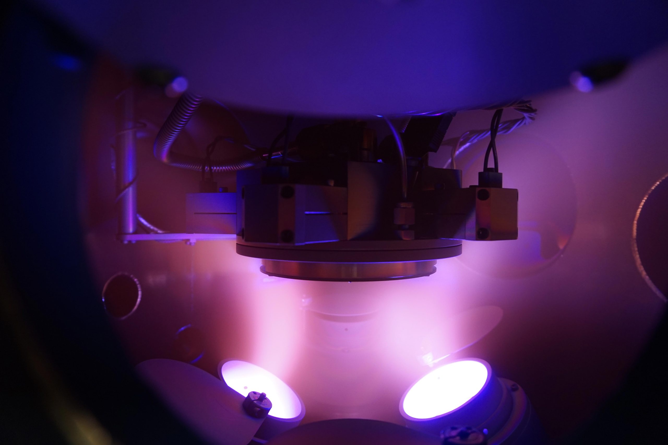
The researchers used a common technique called HiPIMS – short for high power impulse magnetron sputtering – as their starting point. Magnetron sputtering is a coating process in which material is deposited from a solid precursor material – the target – onto the component to be coated – the substrate. To achieve this, a process-gas plasma is ignited at the target. The process-gas ions – usually argon – are then shot at the target, knocking out atoms that subsequently land on the substrate to form the desired thin film. Many materials can be used as targets. For piezoelectric applications, metals are commonly used, often with the addition of nitrogen to produce nitrides such as aluminum nitride.
HiPIMS works in almost the same way – except that the process does not take place continuously, but in short, high-energy pulses. This not only means that the ejected target atoms travel faster – many of them are also ionized on their way through the plasma. This makes the process interesting for research. In contrast to neutral atoms, ions can be accelerated, for example by applying a negative voltage to the substrate. Over the past 20 years or so, this approach has been used to produce hard coatings, with the high energies resulting in especially dense and durable layers.
However, until now, this process was not viable for piezoelectric thin films. This is because applying a voltage to the substrate does not only accelerate the film-forming target ions, but also argon ions from the process gas. This argon bombardment must be avoided. “Several percent of argon can sometimes be incorporated in hard coatings,” says Empa researcher Sebastian Siol. ”Piezoelectric thin films often operate under high voltages. Here, such impurities could lead to a catastrophic electrical breakdown.”
Nevertheless, Siol’s team believed in the potential of HiPIMS for piezoelectric thin films. The high energy with which the ions fly towards the substrate is extremely advantageous. If the ion hits the substrate with sufficient energy, it remains mobile for a short time and can find an optimal position in the growing crystal lattice. But what can be done about the undesired argon inclusions?
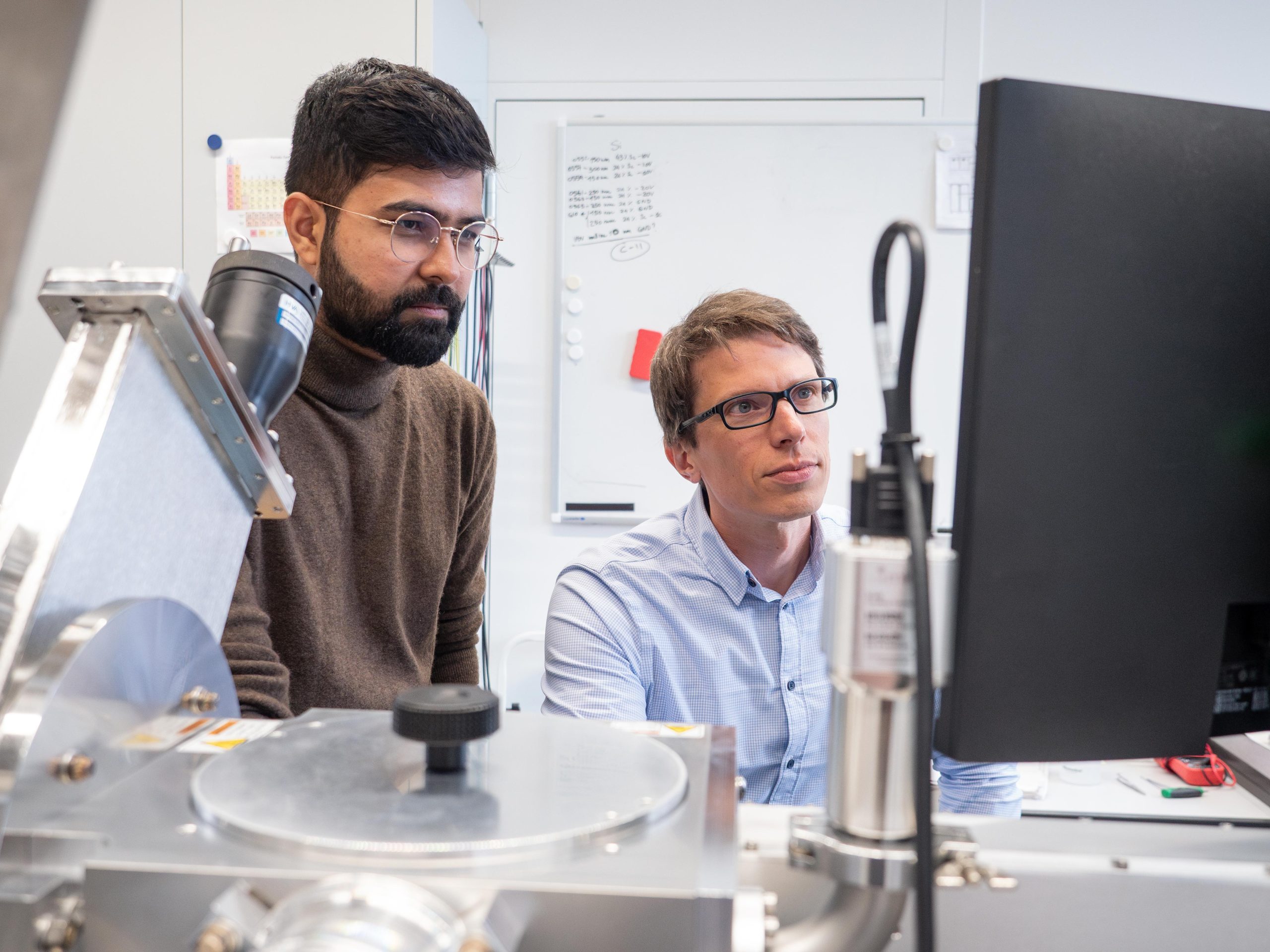
During his doctoral thesis, Jyotish Patidar developed a clever solution. Not all ions arrive at the target at the same time. The majority of argon ions are located in the plasma in front of the target. This means that they often reach the substrate before the target ions, which first must be knocked out of the target and then have to cross the entire distance to the substrate. Patidar’s innovation was in the timing: “If we apply the voltage to the substrate at exactly the right moment, we only accelerate the desired ions,” Siol explains. The argon ions have already flown past at this point – and without the additional acceleration, they have too little energy to be incorporated in the growing film.
“Electron shower” as a flight controller
Using this trick, the researchers were able to produce high-quality piezoelectric thin films with HiPIMS for the first time – with a performance equivalent to or even better compared to conventional methods. Now came the next challenge: Depending on the specific application, thin films need to be produced on insulating substrates, such as glass or sapphire. However, if the substrate is non-conductive, no voltage can be applied to it. Although there is a method in industry to accelerate the ions anyway, but this also often leads to argon inclusions in the layer.
This is where the Empa researchers achieved a breakthrough. To accelerate the ions onto the insulating substrate, they use the magnetron pulse itself – the short impulse that shoots the process gas ions onto the target. The plasma in the chamber contains not only ions, but also electrons. Each pulse from the magnetron automatically accelerates these negatively charged elemental particles onto the substrate. The tiny electrons reach the target much faster than the much larger ions.
Normally, this “electron shower” is not relevant for the HiPIMS process. However, when the electrons arrive at the substrate, for a fraction of a second, they give it a negative charge – enough to accelerate the ions. If the researchers trigger a subsequent magnetron pulse at exactly the right time interval, the electron shower accelerates the target ions that started their flight during the previous pulse. And of course, the timing can also be adjusted so that only the right ions end up in the thin film.
From chips to qubits
The results are impressive: “With our method, we were able to produce piezoelectric thin films on insulating substrates just as well as on conductive ones,” summarizes Siol. The researchers have termed the process Synchronized Floating Potential HiPIMS, or SFP-HiPIMS for short. The big advantage: With SFP-HiPIMS, piezoelectric thin films can be produced in very high quality at low temperatures. This opens up new possibilities for the production of chips and electronic components, which often cannot withstand high temperatures. The technique for insulating substrates is particularly important for the semiconductor industry: “Many production tools in the semiconductor industry are designed in such a way that there is not even a possibility to apply an electrical voltage to the substrate,” says Siol.
In the next step, he aims to work on the development of ferroelectric thin films with his team – another key technology in current and future electronics. Based on this success, the Empa researchers are also launching several collaborations with other research institutions to bring their thin films into applications ranging from photonics to quantum technologies. And finally, they want to further optimize the innovative process with the help of machine learning and high-throughput experiments.
Reference: “Low temperature deposition of functional thin films on insulating substrates enabled by selective ion acceleration using synchronized floating potential HiPIMS” by Jyotish Patidar, Oleksandr Pshyk, Kerstin Thorwarth, Lars Sommerhäuser and Sebastian Siol, 21 May 2025, Nature Communications.
DOI: 10.1038/s41467-025-59911-y
Never miss a breakthrough: Join the SciTechDaily newsletter.
Follow us on Google and Google News.
1 Comment
Ebeam deposition. Ultra high vacuum, no gas, with biased substrate holder.