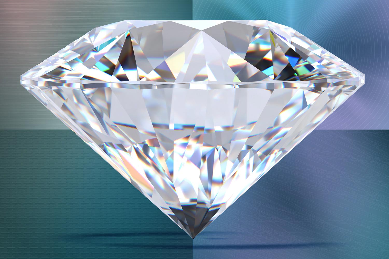
Normally an insulator, diamond becomes a metallic conductor when subjected to large strain in a new theoretical model.
Long known as the hardest of all natural materials, diamonds are also exceptional thermal conductors and electrical insulators. Now, researchers have discovered a way to tweak tiny needles of diamond in a controlled way to transform their electronic properties, dialing them from insulating, through semiconducting, all the way to highly conductive, or metallic. This can be induced dynamically and reversed at will, with no degradation of the diamond material.
The research, though still at an early proof-of-concept stage, may open up a wide array of potential applications, including new kinds of broadband solar cells, highly efficient LEDs and power electronics, and new optical devices or quantum sensors, the researchers say.
Their findings, which are based on simulations, calculations, and previous experimental results, were published on October 5, 2020, in the Proceedings of the National Academy of Sciences. The paper is by MIT Professor Ju Li and graduate student Zhe Shi; Principal Research Scientist Ming Dao; Professor Subra Suresh, who is president of Nanyang Technological University in Singapore as well as former dean of engineering and Vannevar Bush Professor Emeritus at MIT; and Evgenii Tsymbalov and Alexander Shapeev at the Skolkovo Institute of Science and Technology in Moscow.
The team used a combination of quantum mechanical calculations, analyses of mechanical deformation, and machine learning to demonstrate that the phenomenon, long theorized as a possibility, really can occur in nanosized diamond.
The concept of straining a semiconductor material such as silicon to improve its performance found applications in the microelectronics industry more than two decades ago. However, that approach entailed small strains on the order of about 1 percent. Li and his collaborators have spent years developing the concept of elastic strain engineering. This is based on the ability to cause significant changes in the electrical, optical, thermal, and other properties of materials simply by deforming them — putting them under moderate to large mechanical strain, enough to alter the geometric arrangement of atoms in the material’s crystal lattice, but without disrupting that lattice.
In a major advance in 2018, a team led by Suresh, Dao, and Yang Lu from the City University of Hong Kong showed that tiny needles of diamond, just a few hundred nanometers across, could be bent without fracture at room temperature to large strains. They were able to repeatedly bend these nanoneedles to tensile strain as much as 10 percent; the needles can then return intact to their original shape.
Key to this work is a property known as bandgap, which essentially determines how readily electrons can move through a material. This property is thus key to the material’s electrical conductivity. Diamond normally has a very wide bandgap of 5.6 electron volts, meaning that it is a strong electrical insulator that electrons do not move through readily. In their latest simulations, the researchers show that diamond’s bandgap can be gradually, continuously, and reversibly changed, providing a wide range of electrical properties, from insulator through semiconductor to metal.
“We found that it’s possible to reduce the bandgap from 5.6 electron volts all the way to zero,” Li says. “The point of this is that if you can change continuously from 5.6 to 0 electron volts, then you cover all the range of bandgaps. Through strain engineering, you can make diamond have the bandgap of silicon, which is most widely used as a semiconductor, or gallium nitride, which is used for LEDs. You can even have it become an infrared detector or detect a whole range of light all the way from the infrared to the ultraviolet part of the spectrum.”
“The ability to engineer and design electrical conductivity in diamond without changing its chemical composition and stability offers unprecedented flexibility to custom-design its functions,” says Suresh. “The methods demonstrated in this work could be applied to a broad range of other semiconductor materials of technological interest in mechanical, microelectronics, biomedical, energy, and photonics applications, through strain engineering.”
So, for example, a single tiny piece of diamond, bent so that it has a gradient of strain across it, could become a solar cell capable of capturing all frequencies of light on a single device — something that currently can only be achieved through tandem devices that couple different kinds of solar cell materials together in layers to combine their different absorption bands. These might someday be used as broad-spectrum photodetectors for industrial or scientific applications.
One constraint, which required not only the right amount of strain but also the right orientation of the diamond’s crystalline lattice, was to prevent the strain from causing the atomic configuration to cross a tipping point and turn into graphite, the soft material used in pencils.
The process can also make diamond into two types of semiconductors, either “direct” or “indirect” bandgap semiconductors, depending on the intended application. For solar cells, for example, direct bandgaps provide a much more efficient collection of energy from light, allowing them to be much thinner than materials such as silicon, whose indirect bandgap requires a much longer pathway to collect a photon’s energy.
The process could be relevant for a wide variety of potential applications, Li suggests, such as for highly sensitive quantum-based detectors that use defects and dopant atoms in a diamond. “Using strain, we can control the emission and absorption levels of these point defects,” he says, allowing novel ways of controlling their electronic and nuclear quantum states.
But given the great variety of conditions made possible by the different dimensions of strain variations, Li says, “if we have a particular application in mind, then we could optimize toward that application target. And what is nice about the elastic straining approach is that it is dynamic,” so that it can be continuously varied in real time as needed.
This early-stage proof-of-concept work is not yet at the point where they can begin to design practical devices, the researchers say, but with the ongoing research they expect that practical applications could be possible, partly because of promising work being done around the world on the growth of homogeneous diamond materials.
Reference: “Metallization of diamond” by Zhe Shi, Ming Dao, Evgenii Tsymbalov, Alexander Shapeev, Ju Li and Subra Suresh, 5 October 2020, Proceedings of the National Academy of Sciences.
DOI: 10.1073/pnas.2013565117
The work was supported by the U.S. Office of Naval Research.
Never miss a breakthrough: Join the SciTechDaily newsletter.
Follow us on Google and Google News.
1 Comment
Very Interesting.
Possible suggestions for Strain Engineering.
1. Look at Other Crytaline material rather than the expensive a relatively rare version of Carbon which retain their Crystaline Structure and allow such applications to be made a practical relity. There should be such materail existing in nature in plenty and make the Theory and Industrial Use Practical Reality. Not just in the Vertical column No. 14 of the periodic table, but others as well which may change their property across the desirable range of the light spectrum.
2. Just like Cold Fusion , the theoritical possibility exiists that these materials can exist or can be created for industrial use to covert Theory to a Practical Reality on a large sacle for the uses envisioned.