Close Menu
    Facebook X (Twitter) Instagram
    SciTechDaily
    • Biology
    • Chemistry
    • Earth
    • Health
    • Physics
    • Science
    • Space
    • Technology
    Facebook X (Twitter) Pinterest YouTube RSS
    SciTechDaily
    Home»Technology»The Atomic Gap That Could Cost the Semiconductor Industry Billions
    Technology

    The Atomic Gap That Could Cost the Semiconductor Industry Billions

    By Vienna University of TechnologyApril 27, 20263 Comments4 Mins Read
    Facebook Twitter Pinterest Telegram LinkedIn WhatsApp Email Reddit
    Share
    Facebook Twitter LinkedIn Pinterest Telegram Email Reddit
    Clean Room Dust Protection Holding Microprocessor Computer Chip
    Ultrathin 2D materials have long been seen as the key to pushing computer chips beyond current limits. But new research reveals a subtle, often overlooked factor that can quietly undermine their performance and reshape which materials are truly viable for future electronics. Credit: Shutterstock

    Promising 2D materials may face an unexpected obstacle at the atomic scale: a tiny gap at their interfaces.

    For decades, the steady shrinking of electronic components has powered faster, more efficient technology. Engineers now hope to push that trend even further with 2D materials, atomically thin sheets that promise unprecedented control at the smallest scales.

    But a new study from TU Wien shows that many of these once promising materials may not work as expected. The issue is not just the material itself. It is also how it interacts with other components. When a 2D material is paired with an insulating layer, a tiny gap forms between them, significantly reducing performance. Identifying which materials avoid this problem could help the semiconductor industry steer clear of costly dead ends.

    It’s not just the material—it’s the interface

    “For many years, researchers have quite rightly been fascinated by the remarkable electronic properties of novel 2D materials such as graphene or molybdenum disulfide,” says Prof. Mahdi Pourfath, who carried out the research together with Prof. Tibor Grasser at TU Wien’s Institute for Microelectronics. “What is often overlooked, however, is that a 2D material alone does not make an electronic device. We also need an insulating layer—usually an oxide. And this is where things become more complicated from a materials science perspective.”

    2D Conductor and a Dielectric Layer
    A 2D-conductor and a dielectric layer: The unavoidable gap in between changes the electronic properties significantly. Credit: TU Wien

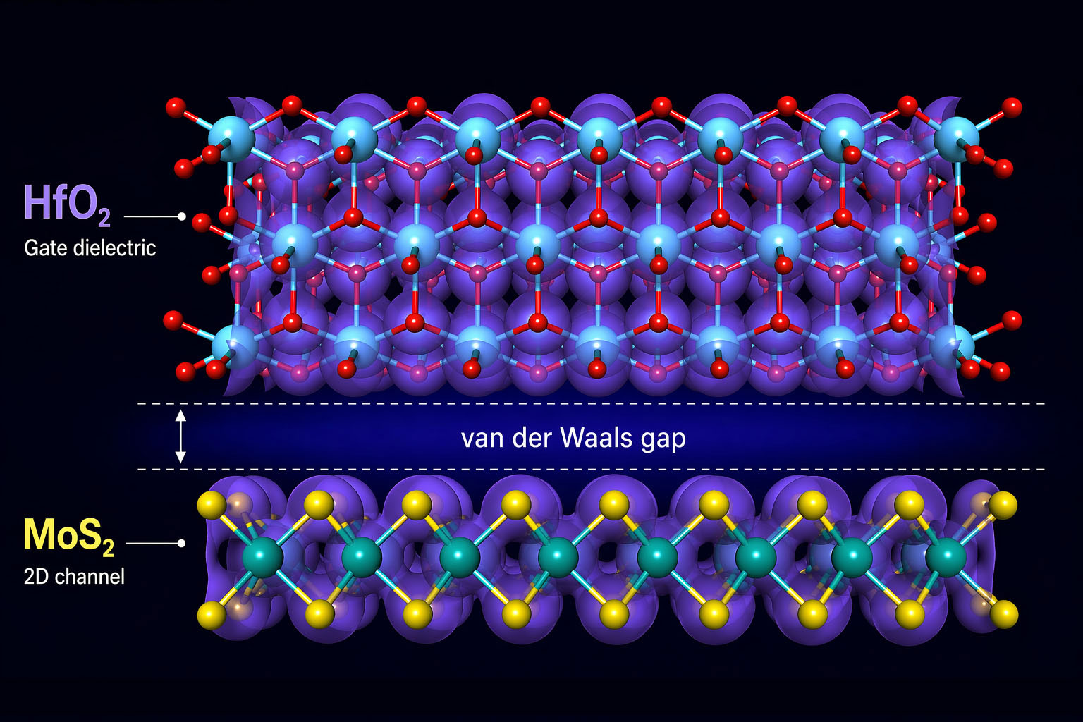
    At their core, transistors operate by switching a semiconductor between conducting and nonconducting states. In this case, the semiconductor can be a 2D material. A gate electrode controls this switching, but it must be separated from the material by an insulating layer.

    Mind the gap!

    To achieve precise control and allow for extremely compact devices, this insulating layer must be as thin as possible. However, atomic-scale analysis reveals a problem that has often been overlooked.

    “In many combinations of 2D materials and insulating layers, the bonding between them is relatively weak,” explains Grasser. “They are held together only by so-called van der Waals forces, which provide only a weak attraction between the semiconductor and the insulator. As a result, the two layers do not come into close contact—there is always a gap between them.”

    This gap is incredibly small, about 0.14 nanometers (0.0000000055 inches), thinner than a single sulfur atom, yet it has a major effect on performance. For comparison, a SARS-CoV-2 virus is about 700 times larger. “This gap weakens the capacitive coupling between the layers. No matter how good the intrinsic properties of the materials may be, the gap can become the limiting factor. As long as it exists, it imposes a fundamental limit on how far these devices can be miniaturized.”

    The solution: “zipper” materials

    “If the semiconductor industry wants to succeed with 2D materials, the active layer and the insulating layer must be designed together from the very beginning,” emphasizes Mahdi Pourfath. One potential solution is the use of “zipper materials,” in which the semiconductor and insulator interlock. Instead of being loosely held together by van der Waals forces, they form a stronger bond that removes the gap.

    “Our work is good news for the semiconductor industry,” says Tibor Grasser. “We can predict which materials are suitable for future miniaturization steps—and which are not. But if one focuses only on the 2D materials themselves, without considering the unavoidable insulating layers from the outset, there is a risk of investing billions in an approach that simply cannot succeed for fundamental physical reasons.”

    Reference: “Device-scaling constraints imposed by the van der Waals gap formed in two-dimensional materials” by Mahdi Pourfath and Tibor Grasser, 16 April 2026, Science.
    DOI: 10.1126/science.aeb2271

    Never miss a breakthrough: Join the SciTechDaily newsletter.
    Follow us on Google and Google News.

    Electronics Materials Science Nanotechnology Popular Semiconductors Vienna University of Technology
    Share. Facebook Twitter Pinterest LinkedIn Email Reddit

    Related Articles

    Invisible to the Human Eye: Scientists Create the World’s Smallest QR Code

    The 1950s Material Making a Massive Comeback To Transform Modern Computing

    The “Electron Shower” That’s Revolutionizing Microchip Manufacturing

    Scientists Unlock New Flexible Semiconductor Using Atomic “Vacancy Engineering”

    Revolutionary 3D Printing Technology a “Game Changer” for Discovering and Manufacturing New Materials

    Physicists Solve a Perplexing Nano-Scale Mystery That Could Help Prevent Overheating in Electronics

    “Mount Everest” of Electronic Materials: Stretching Diamond for Next-Generation Microelectronics

    Smarter Artificial Intelligence Technology in a New Light-Powered Chip

    Turning Diamond Into Metal – For Improved Solar Cells, LEDs, and Power Electronics

    3 Comments

    1. AGEAZIT EMBAYE on April 28, 2026 7:31 pm

      THE FOLLOWING DUE TO THEORIES N THE DISCOVERIES TO COMPLETE THE PYTHEPOEM THEORY IS REVISED FORTHE NEW WORLD FOR ALL THE MORE INCREASED THEORIES ARE VALID INCLUDES A SIMPLE REPETIVE COMMUNICATIONS VARIOUS INCRASED RESULTS I (SCIENCE/MATH/HISTORY/RELIGION/WORLD-LANGUAGES & TELECOMUNICATIONS(WORLD-TECHNOLOGY)INTO THESE COMPRENSIONS ARE DESCRIPTIONS NOT ISSUES ARE DEFINED AREAS OF ALL OF THESE COLLECTONS ARE DEFINED AND REVISED INTO THESE QUESTIONS ARE VALID.

      Reply
    2. Steve Nordquist on April 30, 2026 10:47 pm

      More punctuation, maybe!
      Can’t name it Bloch hand-waving v. smol.

      Reply
    3. Rashad Zaguia on May 2, 2026 2:34 am

      Add another layer having the same gap before removing the resine.
      Connect the top layer using chemistry and electricity on a side and the other of the gap.
      Add your isolation layer leaving a lower layer gap.

      (Removing the resine after adding the isolation layer may not work…)

      No discrimination over names (not bad mahdi !). With my best wishes for no discrimination over color.

      Reply
    Leave A Reply Cancel Reply

    • Facebook
    • Twitter
    • Pinterest
    • YouTube

    Don't Miss a Discovery

    Subscribe for the Latest in Science & Tech!

    Trending News

    New Pill Lowers Stubborn Blood Pressure and Protects the Kidneys

    Humans May Have Hidden Regenerative Powers, New Study Suggests

    Scientists Just Solved the Mystery of Why Crabs Walk Sideways

    Doctors Are Surprised by What This Vaccine Is Doing to the Heart

    This Popular Supplement May Boost Your Brain, Not Just Your Muscles

    Scientists Say This Simple Supplement May Actually Reverse Heart Disease

    Warming Oceans Could Trigger a Dangerous Methane Surge

    This Simple Movement Could Be Secretly Cleaning Your Brain

    Follow SciTechDaily
    • Facebook
    • Twitter
    • YouTube
    • Pinterest
    • Newsletter
    • RSS
    SciTech News
    • Biology News
    • Chemistry News
    • Earth News
    • Health News
    • Physics News
    • Science News
    • Space News
    • Technology News
    Recent Posts
    • Scientists Discover Cheap Material That Kills Deadly Superbugs
    • This Magnetic Field Trick Creates Entirely New Forms of Matter
    • Astronomers Stunned by Ancient Galaxy With No Spin
    • Physicists May Be on the Verge of Discovering “New Physics” at CERN
    • AI Learns To Work Backward and Reveal Hidden Forces in Nature
    Copyright © 1998 - 2026 SciTechDaily. All Rights Reserved.
    • Science News
    • About
    • Contact
    • Editorial Board
    • Privacy Policy
    • Terms of Use

    Type above and press Enter to search. Press Esc to cancel.