

Close Menu
    Facebook X (Twitter) Instagram
    SciTechDaily
    • Biology
    • Chemistry
    • Earth
    • Health
    • Physics
    • Science
    • Space
    • Technology
    Facebook X (Twitter) Pinterest YouTube RSS
    SciTechDaily
    Home»Technology»The 1950s Material Making a Massive Comeback To Transform Modern Computing
    Technology

    The 1950s Material Making a Massive Comeback To Transform Modern Computing

    By University of WarwickNovember 27, 2025No Comments3 Mins Read
    Facebook Twitter Pinterest Telegram LinkedIn WhatsApp Email Reddit
    Share
    Facebook Twitter LinkedIn Pinterest Telegram Email Reddit
    Fastest Charge Carrier Ever on a Silicon Wafer
    Artistic sketch of the fastest charge carrier ever on a silicon wafer (cs-GoS). Credit: Maksym Myronov / University of Warwick

    Researchers are investigating hole mobility in compressively strained germanium on silicon to improve the performance of next-generation electronics.

    Scientists from the University of Warwick and the National Research Council of Canada have set a new record by creating and measuring the highest “hole mobility” ever observed in a material that works with standard silicon technology.

    Today’s semiconductor devices are typically built from Silicon (Si). As these components become increasingly compact and tightly packed, they generate more heat and begin to approach fundamental performance limits. Germanium (Ge), which appeared in some of the earliest transistors of the 1950s, is gaining renewed attention as researchers look for ways to take advantage of its stronger electronic performance while still relying on the well-established manufacturing methods used for silicon.

    According to a new study published in Materials Today, a research group headed by Warwick’s Dr. Maksym Myronov has taken an important step toward future electronic systems. The team developed a nanometer-thin germanium layer that is compressively strained and grown on silicon, resulting in a material that lets electrical charge travel faster than ever before while remaining fully compatible with current chip production processes.

    Maksym Myronov, Associate Professor and leader of the Semiconductors Research Group, Department of Physics, University of Warwick, says, “Traditional high-mobility semiconductors such as gallium arsenide (GaAs) are very expensive and impossible to integrate with mainstream silicon manufacturing. Our new compressively strained germanium-on-silicon (cs-GoS) quantum material combines world-leading mobility with industrial scalability — a key step toward practical quantum and classical large-scale integrated circuits.”
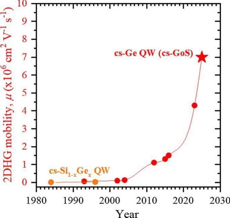
    Hole Mobility for New Germanium Material
    Graphical Abstract demonstrating the hole mobility for new material nanometers-thin compressively strained germanium layer epitaxially grown on a silicon substrate. Hole mobility in compressively strained germanium on silicon exceeds 7× 106 cm2V-1s− 1 . Credit: Myronov, M., Bogan, A., & Studenikin, S. (2025). Hole mobility in compressively strained germanium on silicon exceeds 7× 106 cm2V-1s− 1. Materials Today.

    Engineering Ultra-Clean Germanium on Silicon

    The breakthrough was achieved by carefully engineering a thin germanium layer on top of a silicon wafer. By applying just the right amount of strain to the germanium layer, they created an ultra-clean crystal structure that allows electrical charge to flow almost without resistance.

    When evaluated, the material demonstrated a record hole mobility of 7.15 million cm2 per volt-second (compared to ~450 cm2 per volt-second in industrial silicon), meaning charge can move through it far more easily than in silicon. This could enable future chips to run faster and dissipate less energy.

    Dr. Sergei Studenikin, Principal Research Officer, National Research Council of Canada, adds: “This sets a new benchmark for charge transport in group-IV semiconductors – the materials at the heart of the global electronics industry. It opens the door to faster, more energy-efficient electronics and quantum devices that are fully compatible with existing silicon technology.”

    The research establishes a new pathway for ultra-fast, low-power electronics, with potential applications spanning quantum information processing, spin qubits, cryogenic controllers for quantum processors, AI, and data center hardware with reduced energy and cooling demands.

    Reference: “Hole mobility in compressively strained germanium on silicon exceeds 7 × 106 cm2V-1s−1” by Maksym Myronov, Alex Bogan and Sergei Studenikin, 8 October 2025, Materials Today.
    DOI: 10.1016/j.mattod.2025.10.004

    Funding: EPSRC, National Research Council’s Quantum Sensors Challenge Programme

    Never miss a breakthrough: Join the SciTechDaily newsletter.
    Follow us on Google and Google News.

    Electronics Nanotechnology Popular Semiconductors University of Warwick
    Share. Facebook Twitter Pinterest LinkedIn Email Reddit

    Related Articles

    The Atomic Gap That Could Cost the Semiconductor Industry Billions

    Engineering Breakthrough Paves Way for Chip Components That Could Serve As Both RAM and ROM

    “Mount Everest” of Electronic Materials: Stretching Diamond for Next-Generation Microelectronics

    Smarter Artificial Intelligence Technology in a New Light-Powered Chip

    Turning Diamond Into Metal – For Improved Solar Cells, LEDs, and Power Electronics

    Transistor-Integrated Microfluidic Cooling for More Powerful Electronic Chips

    Order From Disorder: Harnessing Turbulence in Light to Create a High-Precision Laser

    Revolutionary Light-Emitting Silicon – “Holy Grail” Breakthrough After 50 Years of Work

    Dissolvable Electronic Components Could Be Used in Medical Implants

    Leave A Reply Cancel Reply

    • Facebook
    • Twitter
    • Pinterest
    • YouTube

    Don't Miss a Discovery

    Subscribe for the Latest in Science & Tech!

    Trending News

    A Billion Years Before the Grand Canyon, a Giant Cliff May Have Stretched Across America

    The Immune Systems of 110-Year-Olds Are Hiding a Remarkable Secret

    Common Osteoarthritis Treatment Fails a Major Test

    Dark Stars May Have Left a Gravitational-Wave Signal We Can Detect Today

    Blackbirds Somehow Know When a Snake Is Too Dangerous To Attack

    A Hidden Gut Reaction May Explain Why Vegetables Are So Good for You

    New “Invisible” Cell Therapy Could Provide Side-Effect-Free Diabetes Treatment

    Nanoscale “Defects” Unlock a Major Heat Transfer Breakthrough

    Follow SciTechDaily
    • Facebook
    • Twitter
    • YouTube
    • Pinterest
    • Newsletter
    • RSS
    SciTech News
    • Biology News
    • Chemistry News
    • Earth News
    • Health News
    • Physics News
    • Science News
    • Space News
    • Technology News
    Recent Posts
    • NASA’s New Space Telescope Could Map the Entire Sky With Hubble-Like Detail
    • Hidden Deep Beneath Mars, Scientists Find Evidence of a Vast Magmatic System
    • One Tiny Chemical Difference in RNA Could Help Explain the Origins of Life
    • Your Gut Microbiome May Be Contagious, Scientists Discover
    • New Drug Combination Shows Promise Against Advanced Prostate Cancer
    Copyright © 1998 - 2026 SciTechDaily. All Rights Reserved.
    • Science News
    • About
    • Contact
    • Editorial Board
    • Privacy Policy
    • Terms of Use

    Type above and press Enter to search. Press Esc to cancel.