
New TFETs realized with multi-layered in-plane transition metal dichalcogenide junctions.
Tokyo Metropolitan University scientists engineered multi-layered in-plane TMDC junctions with potential use in ultra-low power consumption TFETs, a scalable breakthrough for energy-efficient electronic devices.
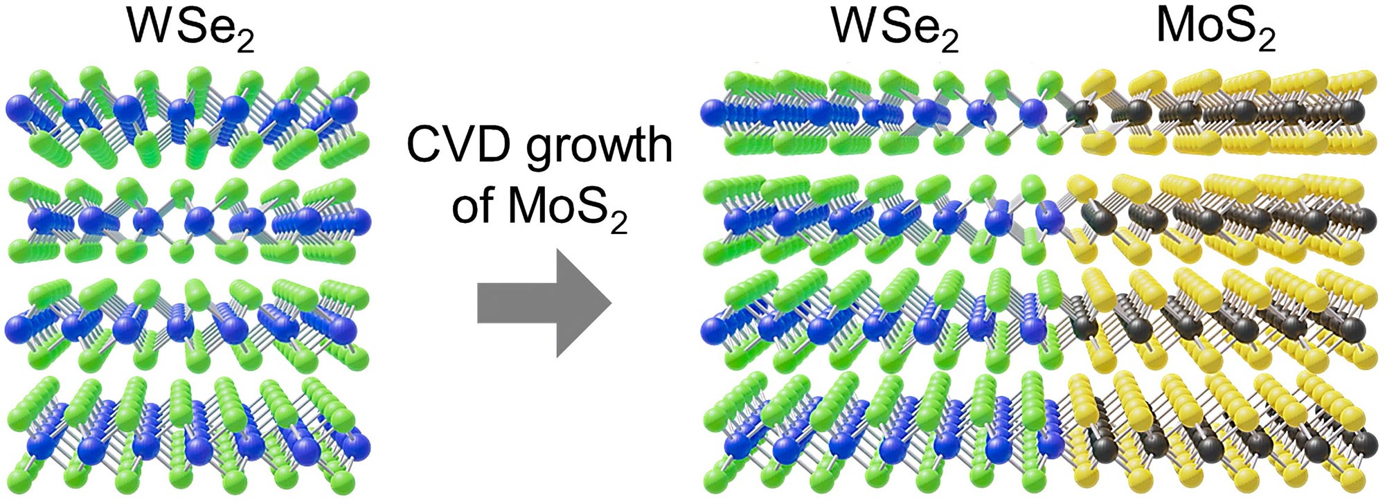
Scientists from Tokyo Metropolitan University have successfully engineered multi-layered nanostructures of transition metal dichalcogenides that meet in-plane to form junctions. They grew out layers of multi-layered structures of molybdenum disulfide from the edge of niobium-doped molybdenum disulfide shards, creating a thick, bonded, planar heterostructure. They demonstrated that these may be used to make new tunnel field-effect transistors (TFET), components in integrated circuits with ultra-low power consumption.
Field-effect transistors (FETs) are a crucial building block of nearly every digital circuit. They control the passage of current through it depending on the voltage which is put across. While metal oxide semiconductor FETs (or MOSFETs) form the majority of FETs in use today, the search is on for the next generation of materials to drive increasingly demanding and compact devices using less power. This is where tunneling FETs (or TFETs) come in. TFETs rely on quantum tunneling, an effect where electrons are able to pass usually impassable barriers due to quantum mechanical effects. Though TFETs use much less energy and have long been proposed as a promising alternative to traditional FETs, scientists are yet to come up with a way of implementing the technology in a scalable form.
Breakthrough in Multi-Layered TMDC Junctions
Led by Associate Professor Yasumitsu Miyata, a team of scientists from Tokyo Metropolitan University has been working on making nanostructures out of transition metal dichalcogenides, a mixture of transition metals and group 16 elements. Transition metal dichalcogenides (TMDCs, two chalcogen atoms to one metal atom) are excellent candidate materials for creating TFETs. Their recent successes have allowed them to stitch together single-atom-thick layers of crystalline TMDC sheets over unprecedented lengths.
Now, they have turned their attention to the multi-layered structures of TMDCs. By using a chemical vapor deposition (CVD) technique, they showed that they could grow out a different TMDC from the edge of stacked crystalline planes mounted on a substrate. The result was an in-plane junction that was multiple layers thick. Much of the existing work on TMDC junctions use monolayers stacked on top of each other; this is because, despite the superb theoretical performance of in-plane junctions, previous attempts could not realize the high hole and electron concentrations required to make a TFET work.
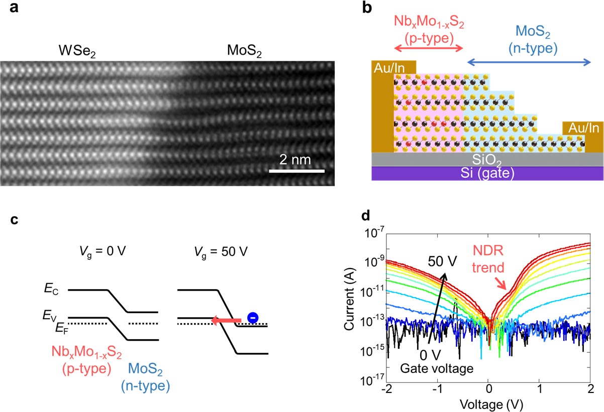
After demonstrating the robustness of their technique using molybdenum disulfide grown from tungsten diselenide, they turned their attention to niobium doped molybdenum disulfide, a p-type semiconductor. By growing out multi-layered structures of undoped molybdenum disulfide, an n-type semiconductor, the team realized a thick p-n junction between TMDCs with unprecedentedly high carrier concentration. Furthermore, they found that the junction showed a trend of negative differential resistance (NDR), where increases in voltage lead to less and less increased current, a key feature of tunneling and a significant first step for these nanomaterials to make their way into TFETs.
The method employed by the team is also scalable over large areas, making it suitable for implementation during circuit fabrication. This is an exciting new development for modern electronics, with hope that it will find its way into applications in the future.
Reference: “Multilayer In-Plane Heterostructures Based on Transition Metal Dichalcogenides for Advanced Electronics” by Hiroto Ogura, Seiya Kawasaki, Zheng Liu, Takahiko Endo, Mina Maruyama, Yanlin Gao, Yusuke Nakanishi, Hong En Lim, Kazuhiro Yanagi, Toshifumi Irisawa, Keiji Ueno, Susumu Okada, Kosuke Nagashio and Yasumitsu Miyata, 23 February 2023, ACS Nano.
DOI: 10.1021/acsnano.2c11927
This work was supported by JSPS KAKENHI Grants-in-Aid, Grant Numbers JP20H02605, JP21H05232, JP21H05233, JP21H05234, JP21H05237, JP22H00280, JP22H04957, JP22H05469, JP22J14738, JP21K14484, JP20K22323, JP20H00316, JP20H02080, JP20K05253, JP20H05664, JP18H01822, JP21K04826, JP22H05445, and JP21K14498, CREST Grant Number JPMJCR16F3 and Japan Science and Technology Agency FOREST Grant Number JPMJFR213X.
Never miss a breakthrough: Join the SciTechDaily newsletter.
Follow us on Google and Google News.
1 Comment
I have recently read an article in Physics.org (edge of chaos)that breaks down the uses of nanowires to develop pathways for intelligent thinking the learning of a brain like neuropathway for remembering past influences, actions and intellects. My thought is how a human forms brain neuropaths from conception threw life, at birth our first pathways imprint is crying that we set at the function to cry as a signal for wanting some thing, we have not yet learned or set a pathway of how to communicate what it is we want, the same as feeding our selves or standing and walking pathways needed for manipulation of mussels. Low energy pathways as in this article for nanostructures at ultra-low power if the two technologies combine for quantum intelligent computing we may find that the same path building would advance a thought process for what we call artificial intelligent computers, then apply to robotic function, teaching the brain to form neuropathway settings. The collaboration between academics would set a pathway for advancement.