A long-standing mystery in materials science is beginning to unravel as researchers directly probe the hidden atomic complexity of relaxor ferroelectrics.
Relaxor ferroelectrics have been used for decades in technologies such as ultrasound equipment, microphones, and sonar systems. Their unusual behavior is rooted in their atomic structure, but researchers have long been unable to measure that structure directly.
A research team from MIT and other institutions has now mapped the three-dimensional atomic structure of a relaxor ferroelectric for the first time. The results, published in Science, could help improve the models used to design future computing, energy, and sensing technologies.
“Now that we have a better understanding of exactly what’s going on, we can better predict and engineer the properties we want materials to achieve,” says corresponding author James LeBeau, MIT’s Kyocera Professor of Materials Science and Engineering. “The research community is still developing methods to engineer these materials, but in order to predict the properties those materials will have, you have to know if your model is right.”
Revealing Hidden Atomic Structure
In the study, the researchers used an emerging imaging method to examine how electric charges are distributed inside the material. What they found challenged earlier assumptions.
“We realized the chemical disorder we observed in our experiments was not fully considered previously,” says co-first authors Michael Xu PhD ’25 and Menglin Zhu, who are both postdocs at MIT. “Working with our collaborators, we were able to merge the experimental observations with simulations to refine the models and better predict what we see in experiments.”
The paper’s authors include Zhu, Xu, and LeBeau, along with Colin Gilgenbach and Bridget R. Denzer, MIT PhD students in materials science and engineering; Yubo Qi, an assistant professor at the University of Alabama at Birmingham; Jieun Kim, an assistant professor at the Korea Advanced Institute of Science and Technology; Jiahao Zhang, a former PhD student at the University of Pennsylvania; Lane W. Martin, a professor at Rice University; and Andrew M. Rappe, a professor at the University of Pennsylvania.
Probing Disordered Materials
Current simulations suggest that when an electric field is applied to relaxor ferroelectrics, positively and negatively charged atoms interact within tiny regions of the material. These interactions are thought to contribute to the materials’ strong energy storage and sensing abilities. Until now, however, the structure of those regions could not be measured directly.
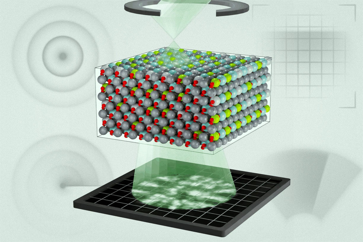
For their Science paper, the team examined a lead magnesium niobate-lead titanate alloy, a relaxor ferroelectric used in sensors, actuators, and defense systems. They studied it with multi-slice electron ptychography (MEP), an emerging technique that scans a nanoscale probe of high-energy electrons across a material and records the electron diffraction patterns that result.
“We do this in a sequential way, and at each position, we acquire a diffraction pattern,” Zhu explains. “That creates regions of overlap, and that overlap has enough information to use an algorithm to iteratively reconstruct three-dimensional information about the object and the electron wave function.”
Insights Across Scales
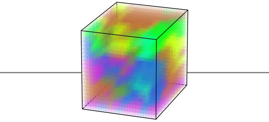
The method exposed layered chemical and polar structures extending from the atomic scale to the mesoscopic scale. It also showed that many areas with different polarization were far smaller than leading simulations had predicted.
The team used those measurements to update computer simulations, making the models better match the material’s behavior under different conditions.
“Previously, these models basically had random regions of polarization, but they didn’t tell you how those regions correlate with each other,” Xu says. “Now we can tell you that information, and we can see how individual chemical species modulate polarization depending on the charge state of atoms.”
Toward Better Materials Design
Zhu says the study highlights electron ptychography as a powerful tool for examining complex materials and could open new paths for studying disordered systems.
“This study is the first time in the electron microscope that we’ve been able to directly connect the three-dimensional polar structure of relaxor ferroelectrics with molecular dynamics calculations,” Xu says. “It further proves you can get three-dimensional information out of the sample using this technique.”
The researchers say the approach may eventually help scientists design materials with advanced electronic properties for improved memory storage, sensing, and energy technologies.
“Materials science is incorporating more complexity into the material design process — whether that’s for metal alloys or semiconductors — as AI has improved and our computational tools have become more advanced,” LeBeau says. “But if our models aren’t accurate enough and we have no way to validate them, it’s garbage in garbage out. This technique helps us understand why the material behaves the way it does and validate our models.”
Reference: “Bridging experiment and theory of relaxor ferroelectrics with multislice electron ptychography” by Menglin Zhu, Michael Xu, Yubo Qi, Colin Gilgenbach, Jieun Kim, Jiahao Zhang, Bridget R. Denzer, Lane W. Martin, Andrew M. Rappe and James M. LeBeau, 30 April 2026, Science.
DOI: 10.1126/science.ads6023
The work was supported, in part, by the U.S. Army Research Laboratory, the U.S. Office of Naval Research, the U.S. Department of War, and a National Science Graduate Fellowship. The researchers also used MIT.nano facilities.
Never miss a breakthrough: Join the SciTechDaily newsletter.
Follow us on Google and Google News.