
Researchers may have unlocked the future of computing by turning flat silicon chips into densely stacked 3D architectures.
For decades, the semiconductor industry has boosted computing power by making transistors smaller and fitting more of them onto a single chip. That strategy has fueled remarkable advances in electronics, but it is now approaching fundamental physical limits. As devices shrink toward atomic scales, engineers must contend with the constraints of material properties and the effects of quantum mechanics.
Researchers believe the next major advance may come not from making chips smaller, but from building them upward.
A team at the University of Illinois Grainger College of Engineering has demonstrated a new way to stack layers of silicon circuits directly on top of one another, creating compact three-dimensional chips that could deliver greater computing power while using less energy. Their work, published in Nature, overcomes a major obstacle that has long prevented widespread adoption of this approach.
“Take something as simple as static random-access memory, which is universal in CPUs and GPUs. Today it takes six microelectronic devices called transistors on a single plane to store one bit of information. With vertical integration, you can distribute them across multiple layers. It’s like replacing a sprawling suburb with high-rises: you get the same functionality, but the spatial footprint is reduced while making communication between layers faster and more efficient,” said Qing Cao, a professor of materials science and engineering at Illinois Grainger Engineering.
Why Computer Chips Need a New Direction
For more than 60 years, the semiconductor industry has followed Moore’s law, the observation that transistor density on a chip roughly doubles every two years. This trend has served as a guiding target for chip manufacturers, enabling steady gains in performance and efficiency.
That progress is becoming increasingly difficult to sustain.
“In a sense, we’re hitting a limit imposed by physics,” Cao said. “If you look at the actual size of transistors, they’re not getting smaller, especially in terms of their contacted gate pitch. This is because we’re becoming limited by the intrinsic material properties of silicon and the fundamental rules of quantum mechanics. If we’re going to keep up the trend of increasing processing power of our microprocessors, we have to start thinking beyond just squeezing more devices on a single surface.”
Instead of continuing to shrink transistors, many researchers see vertical integration as the next logical step. Stacking devices in multiple layers creates additional space for circuitry while shortening the wiring needed to connect components. Shorter connections reduce parasitic capacitance and significantly increase communication bandwidth between devices and circuit blocks.
These advantages are particularly attractive for artificial intelligence and other data-intensive applications that demand ever-increasing computing performance.
Monolithic 3D Chips Offer Major Advantages
Several commercial products already use three-dimensional chip technologies. These systems are typically made by manufacturing semiconductor devices on separate wafers and then bonding them together afterward.
While that method has enabled technologies such as high-bandwidth memory and 3D V-Cache, it has limitations. The alignment between layers is relatively coarse, and the vertical connections known as through-silicon via (TSV) are comparatively large and widely spaced.
Monolithic three-dimensional integration takes a different approach. Instead of stacking completed wafers, each layer is built directly on top of the one beneath it during fabrication.
This strategy allows vertical connections to be 10-100 times denser, reduces the distance between layers, and enables alignment with nanometer-scale precision.
Despite its promise, monolithic integration has remained difficult to achieve in practice because of one major issue: heat.
Solving the Temperature Problem
Producing high-quality crystalline silicon and fabricating advanced semiconductor devices typically requires temperatures approaching 1,000 degrees Celsius. However, the metal wiring already present in lower chip layers cannot withstand such extreme heat.
“Generally, the industry accepts that once the first layer of circuits is complete, the thermal budget limit for any additional layers is 400 degrees Celsius,” Cao said. “Researchers in both academia and industry have tried to get around this by working with semiconductor materials other than single-crystalline silicon for the upper layers. But the resulting devices all inevitably suffer from issues with performance and reliability.”
Previous efforts have explored alternatives including polycrystalline silicon, amorphous or nanocrystalline metal oxides, carbon nanotubes, and two-dimensional semiconductors. However, these materials often introduce performance limitations or processing defects that create a mismatch with the high-performance silicon devices in the lower layers.
The Illinois team developed a different solution that retains industry-standard single-crystalline silicon throughout the structure.
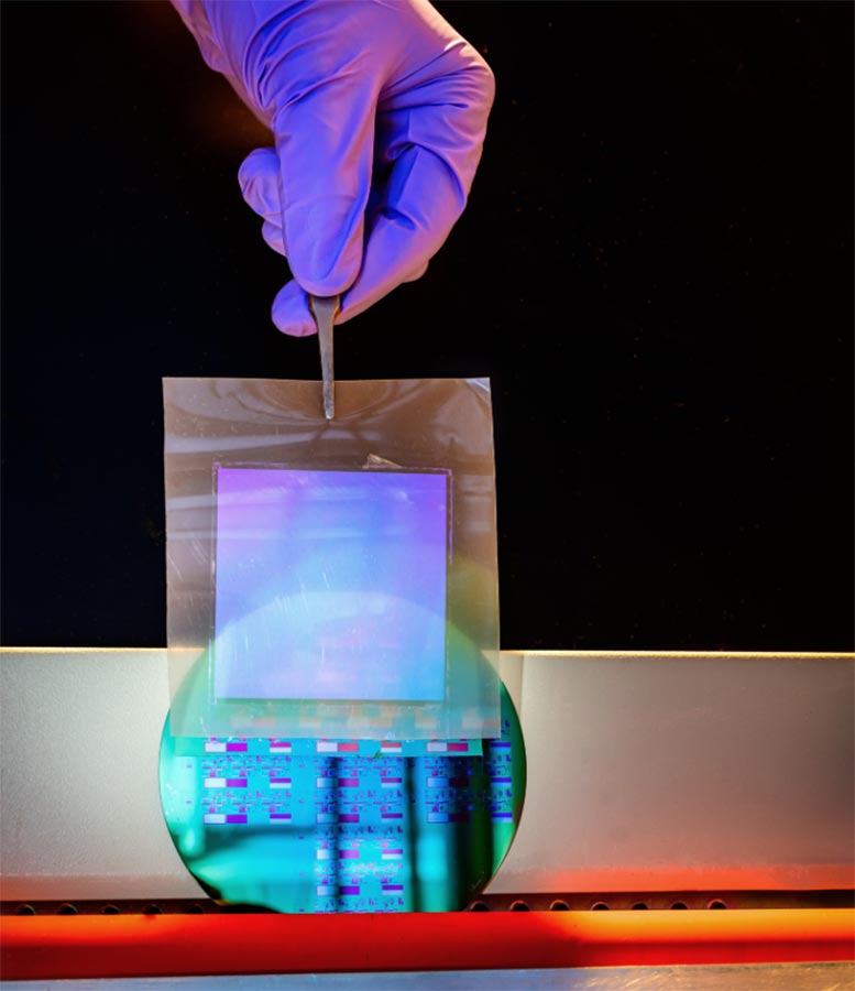
Their method begins by creating ultrathin freestanding silicon nanomembranes from a donor wafer. These membranes are then transferred onto a substrate that already contains completed circuitry using a roll laminator. The bonding process requires temperatures no higher than 200 degrees Celsius, well below the industry’s accepted thermal limit.
Because the silicon remains highly crystalline, the resulting devices maintain strong performance and reliability while avoiding heat damage to lower layers.
“Our method is not only easier to implement with lower cost, but it has several advantages over previous approaches to stack silicon wafers,” Cao said. “The membranes we transferred are only 10 nanometers thick or less, compared to the 500 to 700 micrometers thickness of a typical wafer. Because they are thin, these membranes are mechanically flexible to conform to the underlying surface. This conformality helps avoid interfacial defects like voids, which are common when trying to force two rigid wafers together via wafer bonding.”
Building High Performance Stacked Silicon Circuits
The researchers also redesigned the transistor architecture.
Traditional semiconductor manufacturing relies on a process called doping, which introduces impurities into silicon to control its electrical behavior. This step usually requires temperatures above 600 degrees Celsius, making it unsuitable for monolithic stacking.
To avoid that challenge, the team employed junctionless transistors. In these devices, the silicon is heavily and uniformly doped before stacking occurs. Because the silicon films are extremely thin, the transistor gate can still effectively control the channel, while the high doping concentration helps reduce parasitic contact resistance.
Using their approach, the researchers fabricated three stacked layers containing 625 transistors per layer. The devices demonstrated strong uniformity and high yields.
Performance was also impressive. Output current densities matched those of conventional silicon transistors fabricated on bulk wafers using much higher temperatures and were at least three to four times greater than monolithic devices made from alternative materials.
The team connected the layers using vertical metal lines and successfully demonstrated three-dimensional integrated logic circuits and static random-access memory cells.
Perhaps most importantly, the researchers believe the process can be expanded beyond the three layers demonstrated in the study.
“But most importantly, we’ve shown that this process is scalable,” Cao said. “You can keep stacking layers beyond the three we demonstrated. And the process will yield high-performing transistors with high yield and low variability. We now have a strong foundation for transferring this technology and demonstrating its immediate promise in an industrial semiconductor foundry.”
Toward Commercial 3D Silicon Chips
The researchers reported device yields of 98‒100% even in an academic cleanroom environment, a result that suggests strong potential for industrial manufacturing.
“Vertical integration is already starting to make its way into commercial devices, particularly in specialized AI hardware, but monolithic integration is what unlocks the full promise of 3D chips,” Cao said. “For the first time, we have met the thermal budget of monolithic 3D integration using standard single-crystalline silicon and delivered unprecedented performance.”
Reference: “Monolithic three-dimensional integration of silicon transistors” by Bao Lam, Yung Man Yu, Hyunjun Nam, Hsu-Chih Ni, Shomik Chatterjee, Shaloo Rakheja, Jian-Min Zuo and Qing Cao, 27 May 2026, Nature.
DOI: 10.1038/s41586-026-10496-6
The work was carried out through Illinois Grainger Engineering’s Center for Advanced Semiconductor Chips with Accelerated Performance, whose industry partners include IBM, Intel, and Taiwan Semiconductor Manufacturing Company. The team is now working to transfer the technology to an industrial semiconductor foundry.
Additional contributors to the study included Bao Lam, Yung Man Yu, Hyunjun Nam, Hsu-Chih Ni, Shomik Chatterjee, Shaloo Rakheja, and Jian-Min Zhuo.
Funding was provided by the National Science Foundation, industry partners of Illinois Grainger Engineering’s Center for Advanced Semiconductor Chips with Accelerated Performance, and the Silicon Crossroads Microelectronics Commons Hub.
Never miss a breakthrough: Join the SciTechDaily newsletter.
Follow us on Google and Google News.