Researchers at Münster University develop an easy-to-produce interface between quantum emitters and nanophotonic networks.
Quantum effects are genuinely found in the world of nanostructures and allow a wide variety of new technological applications. For example, a quantum computer could in the future solve problems, which conventional computers need a lot of time to handle. All over the world, researchers are engaged in intensive work on the individual components of quantum technologies – these include circuits that process information using single photons instead of electricity, as well as light sources producing such individual quanta of light. Coupling these two components to produce integrated quantum optical circuits on chips presents a particular challenge.
Researchers at the University of Münster have now developed an interface that couples light sources for single photons with nanophotonic networks. This interface consists of so-called photonic crystals, i.e. nanostructured dielectric materials that can enhance a certain wavelength range when light passes through. Such photonic crystals are used in many areas of research, but they had not previously been optimized for this type of interface. The researchers took particular care to achieve this feat in a way that allows for replicating the photonic crystals straightforwardly by using established nanofabrication processes.
“Our work shows that it is not only in highly specialized laboratories and unique experiments that complex quantum technologies can be produced,” says physicist Dr. Carsten Schuck, an assistant professor at Münster University who headed the study together with Dr. Doris Reiter, likewise an assistant professor, who works in the field of solid state theory. The results could help to make quantum technologies scalable. The study was published in the journal Advanced Quantum Technologies on October 1, 2019.
Background and method:
As single photons obey the laws of quantum physics, researchers talk of quantum emitters with respect to the light sources involved. For their study, the researchers considered quantum emitters which are embedded in nanodiamonds and emit photons when they are stimulated by means of electromagnetic fields. In order to produce the interfaces desired, the researchers’ aim was to develop optical structures tailored to the wavelength of the quantum emitters.
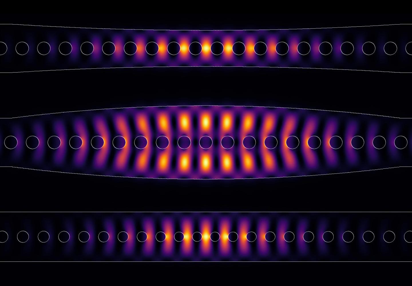
Cavities or holes in photonic crystals are well suited for trapping light in minute volumes and getting it to interact with matter such as, in this case, nanodiamonds. Jan Olthaus, a Ph.D. student in physics in Doris Reiter’s junior research group, developed theoretical concepts and special computer-assisted simulation techniques in order to compute the designs for these photonic crystals.
The theoretically developed designs were produced by physicists in the junior research group headed by Carsten Schuck at the Center for NanoTechnology and the Center for Soft Nanoscience at Münster University. Ph.D. student Philipp Schrinner manufactured the crystals from a thin film of silicon nitride. For this purpose, he used modern electron beam lithography and special etching methods on the equipment at the Münster Nanofabrication Facility and succeeded in producing high-quality crystals directly on the base material of silicon dioxide.
In structuring the crystals, the researchers varied not only the size and the arrangement of the cavities, but also the width of the waveguide on which the cavities were placed. The results measured showed that photonic crystals which demonstrated a special variation in hole sizes were best suited for the interfaces.
“Our collaboration – between theoretical and experimental physicists – is an ideal one for physics research,” says Doris Reiter. “This type of collaboration isn’t always easy, as our respective methods of working are often very different indeed – which is why we are all the more delighted that it turned out so well in the case of our two junior research groups.” “What’s special about our work,” adds Carsten Schuck, “is that our designs don’t require any additional processing steps, because they are compatible with established thin-film technology for integrated photonic circuits.” This cannot be taken for granted in the development of complex quantum technologies, because although researchers often succeed in producing an important, high-quality component as a one-off, they are not able to produce multiple copies of the same component again.
The next steps for the researchers involve trying to position the quantum emitters, embedded in the nanodiamonds, at certain spots on the photonic crystals – with the aim of putting the results of the study into practice. To this end, the team headed by Carsten Schuck is already developing a special nanofabrication technique which is able, for example, to place a diamond just 100-nanometers in size with an accuracy of less than 50 nanometers. The team of theoretical physicists led by Doris Reiter wants to extend the studies to other materials systems and more complex geometries of photonic crystals and, for example, use elliptical holes instead of round ones.
Reference: “Optimal Photonic Crystal Cavities for Coupling Nanoemitters to Photonic Integrated Circuits” by Jan Olthaus, Philip P. J. Schrinner, Doris E. Reiter and Carsten Schuck, 1 October 2019, Advanced Quantum Technologies.
DOI: 10.1002/qute.201900084
The study received funding from the Ministry of Culture and Science of the State of North Rhine-Westphalia.
Never miss a breakthrough: Join the SciTechDaily newsletter.
Follow us on Google and Google News.