Credit: Amy Pan and Sampson Wilcox
A new MIT-designed lidar chip uses specially engineered antennas to reduce interference and widen the sensor’s field of view.
From self-driving cars navigating busy streets to drones surveying disaster zones, lidar has become one of the most important technologies for helping machines perceive the world in three dimensions. By sending out rapid pulses of infrared light and measuring their reflections, lidar systems can build highly detailed maps of their surroundings in real time.
But today’s most powerful lidar sensors often come with major drawbacks: they are bulky, expensive, and rely on moving mechanical components that can wear out over time.
Researchers at MIT have now demonstrated a potential solution. They developed a new silicon-photonics chip that could enable compact, durable lidar systems with no moving parts. Silicon photonics uses semiconductor technology to manipulate light rather than electricity, opening the door to lidar sensors that are smaller, cheaper, and easier to manufacture at scale.
One of the biggest obstacles facing silicon-photonics lidar has been its limited field of view. Existing chip-based systems struggle to scan wide angles, while methods for expanding their coverage typically introduce noise and reduce measurement accuracy.
To overcome this challenge, the MIT team designed an array of integrated antennas that dramatically reduces unwanted interference, known as crosstalk, between neighboring antennas. Their approach allows a lidar chip to scan a much wider area while maintaining the low-noise, high-precision performance needed for demanding applications such as autonomous vehicles, aerial mapping, and construction-site monitoring.
Solid-State Lidar Could Transform Autonomous Navigation
The breakthrough could support the development of advanced lidar sensors for applications such as autonomous driving, aerial surveying, and construction site monitoring.
“The functionality we demonstrated in this work solves a fundamental problem for integrated optical-phased-array technology, enabling future lidar sensors that can achieve significantly higher performance than we could demonstrate previously,” says Jelena Notaros, the Robert J. Shillman Career Development Associate Professor of Electrical Engineering and Computer Science (EECS) at MIT, a member of the Research Laboratory of Electronics, and senior author of a paper on this innovation.
The paper’s lead author is EECS graduate student Henry Crawford-Eng. Additional co-authors include EECS graduate students Andres Garcia Coleto, Benjamin M. Mazur, Daniel M. DeSantis, and Tal Sneh. The findings were published in Nature Communications.
Conventional lidar systems typically rely on a spinning unit that sends light pulses in multiple directions. The reflected light returns to the sensor, allowing the system to reconstruct a map of the environment.
How Silicon-Photonics Lidar Steers Light
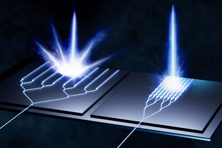
Silicon-photonics lidar systems instead steer light electronically using an integrated optical phased array (OPA), eliminating the need for moving parts.
An OPA contains a series of integrated antennas with tiny periodic corrugations along their surfaces. These corrugations scatter incoming light upward and outward from the photonic chip.
By changing the phase of light sent to each antenna, researchers can control the direction of the emitted beam and steer it electronically.
However, placing antennas too close together creates interference between them, causing the emitted light to become distorted. To avoid this, engineers usually spread the antennas farther apart, but that creates a different problem.
Grating Lobes Restrict Field of View
When antennas are spaced too widely, the array generates multiple copies of the light beam at different angles. As a result, the primary beam can only be steered within a limited range before it becomes indistinguishable from neighboring beams.
“This limits our field of view, so the autonomous vehicle now only knows what is in front of it for a certain angular range,” Garcia Coleto explains.
These duplicate beams, called grating lobes, can confuse the sensor, create false positives, and waste energy.
To solve the issue, the MIT researchers designed reduced-crosstalk antennas that can be placed much closer together without producing significant interference.
MIT’s Reduced-Crosstalk Antenna Innovation
In conventional OPAs, every antenna uses the same geometry and corrugation pattern, causing strong coupling when antennas are tightly packed.
The MIT team addressed this by creating three different antenna designs with varying widths and corrugation arrangements. These differences give each antenna a unique propagation coefficient, which affects how light travels through it.
“Because the antennas have very different propagation coefficients, when we put them close together, essentially each antenna doesn’t ‘see’ the antenna next to it. Therefore, it won’t couple with its neighbor,” Garcia Coleto says.
Even with different propagation characteristics, the antennas still needed to emit light in a uniform way.
Engineering Antennas for Uniform Beam Emission
The researchers carefully engineered the antennas to satisfy three requirements.
Each antenna had to emit the same amount of light, direct the beam at the same angle for a given wavelength, and shift the emission angle consistently as the beam was steered across the array.
“We have this challenge where we require the antennas to have different geometries to reduce the crosstalk, but we need to simultaneously design the antennas to have the same emission characteristics. While it is possible to engineer this, it is extremely difficult because, typically, when antennas are designed with different geometries, they tend to behave differently,” Crawford-Eng says.
The team first developed the electromagnetic theory describing how radiative modes interact, then used those findings to design and simulate the antennas.
Experimental Results Demonstrate Major Performance Gains
Using this approach, the researchers built an OPA with antennas spaced much more closely together than those in traditional systems and then tested the device experimentally.
In a conventional OPA, coupling under similar conditions would reach roughly 100 percent. In the MIT system, coupling dropped to about 1 percent while still producing a single, precise beam. The design also enabled accurate beam steering across a wide field of view without generating grating lobes.
The researchers now plan to improve the technology further to expand the field of view even more. They are also investigating another possible solution for wide-angle functionality that emerged while developing the underlying theory.
“This work addresses a longstanding challenge in integrated optical phased arrays: simultaneously achieving both a wide field of view, which requires dense antenna spacing, and high beam quality, which requires low crosstalk between neighboring antennas. The authors solve this problem with an elegant antenna design. Their innovation is an important step forward for chip-scale, solid-state beam-steering technology,” says Joyce Poon, professor of electrical and computer engineering at the University of Toronto and director of the Max Planck Institute of Microstructure Physics, who was not involved with this work.
Reference: “Reduced-crosstalk antennas for grating-lobe-free and wide-field-of-view integrated optical phased arrays” by Henry Crawford-Eng, Andres Garcia Coleto, Benjamin M. Mazur, Daniel M. DeSantis, Tal Sneh and Jelena Notaros, 7 May 2026, Nature Communications.
DOI: 10.1038/s41467-026-71832-y
This research was supported, in part, by the Semiconductor Research Corporation, the National Science Foundation, an MIT MathWorks Fellowship, the U.S. Department of War, and the MIT Rolf G. Locher Endowed Fellowship.
Never miss a breakthrough: Join the SciTechDaily newsletter.
Follow us on Google and Google News.
9 Comments
An OPA contains a series of integrated antennas with tiny periodic corrugations along their surfaces.
VERY GOOD!
Please ask researchers to think deeply:
1. Where do the tiny periodic corrugations along their surfaces come from?
2. Why is there so much periodicity in the cosmos?
Why is there so much vortex (periodicity and spin) structure in the cosmos? Physical Review Letters, Nature, Science, and Nature Physics—have never earnestly reflected on a fundamental physical question: Where do the things in space come from? Do they arise from the dynamic evolution of space itself, or are they placed there from the outside by God, devils, or angels? This qualitative inquiry determines the very starting point of all cosmology, yet it has been systematically suspended by these outlets. In practice, these publications echo and shield one another. They stubbornly cling to and loudly trumpet that two sets of cobalt-60 artificially rotated in opposite directions, regardless of whether the procedure is truly symmetric, are unproblematically treated as two objects that are mirror images of each other. In the physical world they have constructed, a topological vortex and its twin anti-vortex can even be defined as two vortices possessing entirely different spacetime manifolds (as shown in Figure 3), conveniently ignoring that such a definition already presupposes the qualitative arbitrariness that spacetime can be segmented at will. Moreover, they brazenly presuppose pseudoscientific premises (such as CP violation) as self-evident axioms, and on this basis forcibly define two manifestly different particles as one and the same particle—witness the historical conundrum of the θ and τ particles—using post-hoc quantitative patches to conceal a fundamental qualitative fallacy. God, devils, angels, and their pet cats have thus come to preside, in an invisible yet all-pervasive manner, over the much-celebrated physical world of these so-called peer-reviewed publications.
—— Excerpted from https://zhuanlan.zhihu.com/p/2045049971687391626.
Figure 3:https://pic2.zhimg.com/v2-4127b0b58fe8b88feb27c189fb705029_1440w.jpg?source=172ae18b.
Figure 3:
https://pic2.zhimg.com/v2-4127b0b58fe8b88feb27c189fb705029_1440w.jpg?source=172ae18b.
This picture depicts the construction of natural ‘bricks’. They will create energy gaps when they build themselves. The positive matter and antimatter of science are simultaneous, while the positive matter and antimatter of pseudoscience are sequential. A correct understanding of the relationship between matter and antimatter is crucial for scientific research. From classifying nature to constructing nature, science must respect historical materialism.
Physical Review Letters, Nature, Science, and Nature Physics,have long since degenerated from guardians of the scientific spirit into the custodians of pseudoscience and the gravediggers of science.
—— Excerpted from https://zhuanlan.zhihu.com/p/2045049971687391626.
Some so-called peer-reviewed publications, including Physical Review Letters, Nature, Science, and Nature Physics, please you do not consider shamelessness as noble. The public is not fools. Your blatant waste of public resources is a public insult to the intelligence of the public.
thanks for
Looking at the Wave
This bridges raw math with a physical workbench blueprint. By transforming a flat 2D oscilloscope image into a 3D volumetric corkscrew, it proves that energy doesn’t just travel through a grid—its own rotational signature actively carves out the multi-dimensional track, locking the entire vortex into a perfectly stable, self-drawn structure.
Very good!
This is the transition from classifying nature to constructing nature.