
The discovery could advance integrated photonics, on-chip optical signal transmission, and future quantum technologies.
A nanoscale gold antenna placed on a crystal can send infrared light along one narrow route, even though no physical waveguide has been carved into the material.
Researchers at the 4th Physics Institute of the University of Stuttgart and the Istituto Italiano di Tecnologia (IIT) in Milan demonstrated this mechanism in a naturally hyperbolic van der Waals material. The result could support integrated photonics, optical communication on chips, and future quantum technologies.
Light released from a small source normally spreads outward as circular or spherical wavefronts, much like ripples expanding after a stone strikes water. This uniform propagation is a basic property of waves, but it becomes a problem when photonic devices need to move light efficiently along a specific route.
Modern optical systems solve this problem with waveguides. Glass fibers, for example, confine laser light so it can travel long distances with little loss. Photonic integrated circuits use much smaller waveguides created through lithographic manufacturing steps such as resist coating, lithography, and etching. Producing these nanostructures is technically difficult and adds substantially to manufacturing costs.
Professor Harald Giessen of the 4th Physics Institute of the University of Stuttgart and Dr. Antonio Ambrosio of the Istituto Italiano di Tecnologia (IIT) led a collaboration that demonstrated another way to direct light without manufacturing an artificial waveguide.
Crystal properties create a natural channel
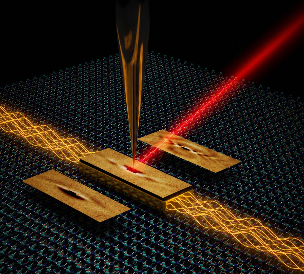
The researchers worked with the two-dimensional material molybdenum oxy-dichloride (MoOCl₂). They positioned a nanoscale gold antenna on its surface and illuminated it with an infrared laser. This generated tightly confined optical waves that moved in only one direction.
Instead of spreading across the material, the light remained within a narrow channel. Its behavior resembled light traveling through an invisible waveguide contained naturally inside the crystal.
Farid Aghashirinov, a doctoral researcher at the 4th Physics Institute, and Andrea Mancini, a postdoctoral fellow at the IIT, conducted the experiments using scattering-type scanning near-field optical microscopy (SNOM). Unlike conventional approaches, the method requires no nanostructuring of the material because the crystal itself determines where the light travels.
MoOCl₂ is a biaxial material, meaning that its optical properties differ sharply along separate crystal directions. Along one axis, it behaves like a metal and supports surface plasmons, which are collective electron oscillations capable of transporting electromagnetic energy.
Along the perpendicular axis, the material behaves as a dielectric and strongly restricts plasmon movement. This extreme directional difference, known as anisotropy, confines the plasmonic waves within a narrow route.
Because the effect resembles water being directed through a canal, the researchers call it plasmon canalization.
Wavelength reshapes how light travels
The shape and direction of the waves changed substantially with the infrared wavelength. At approximately 4 μm, the researchers observed strongly directional canalized propagation.
When they increased the wavelength to 5 μm, the wavefront returned to a familiar ring-like form resembling ripples moving evenly across water. At 3 μm, it instead developed an open hyperbolic shape.
The canalized state can be understood as an elliptical wavefront stretched so far that the ellipse’s focal points effectively move to infinity. By changing only the excitation wavelength, the researchers shifted the propagating waves in MoOCl₂ from an open form to a closed form, passing through the critical canalization state between them.
The experiments used a tunable infrared laser developed by Stuttgart Instruments GmbH, a spin-off company from the University of Stuttgart. The researchers recorded the near-field optical images with a SNOM microscope produced by attocube systems AG, another technology company that emerged from academic research.
Photonic chips could need fewer waveguides
The researchers propose that plasmon canalization in naturally hyperbolic materials could become a new foundation for integrated photonics. Because the material transports light directionally without lithographically manufactured waveguides, it may simplify the production of photonic chips.
The approach could also broaden the available designs for optical interconnects, nanoscale photonic circuits, and integrated quantum technologies.
Reference: “Intrinsic plasmon canalization in the biaxial van der Waals crystal MoOCl2” by Farid Aghashirinov, Andrea Mancini, Lin Nan, Giacomo Venturi, Bettina Frank, Harald Giessen and Antonio Ambrosio, 3 August 2026, Nature Nanotechnology.
DOI: 10.1038/s41565-026-02243-9
Never miss a breakthrough: Join the SciTechDaily newsletter.
Follow us on Google and Google News.
1 Comment
“Guiding infrared light through a crystal without etching a physical channel highlights a broader shift in physics: moving from static structural containers to dynamic medium geometry. Whether it’s controlling photon paths via hyperbolic anisotropy, relaxing bond defects via molten salt flux, or lowering potential barriers via field gradients, the principle remains identical. When you shape the background medium’s directional impedance, the energy naturally channels itself without brute-force constraint.”