
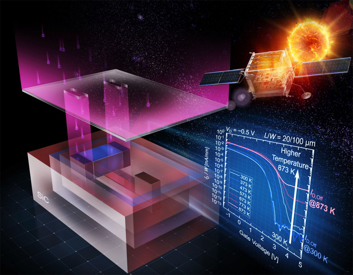
A new bottom gate design takes advantage of the intrinsic properties of SiC.
For more than 20 years, silicon carbide – SiC – has been viewed as a promising material for electronics that must function in extreme environments. Yet despite years of research, that promise has rarely translated into practical devices. Researchers at Kyoto University are now trying to move the field beyond that barrier.
“We believe the lack of development is because the research community has been trying to apply silicon-era thinking to a fundamentally different material,” says first author Mitsuaki Kaneko.
Conventional designs limited SiC performance
The researchers focused on junction field-effect transistors, or JFETs. Earlier work suggested that complementary circuits built from SiC JFETs could provide low-power integrated electronics capable of operating under extreme conditions.
But the group’s previous JFETs, which used conventional top-gate structures fabricated in semi-insulating SiC substrates, had two major shortcomings: poor controllability and substantial leakage current at high temperatures. Solving both problems was considered essential for practical applications.
“Our goal is to open a new path forward with complementary JFETs designed to harness the intrinsic properties of SiC itself,” says Kaneko.
Instead of creating an entirely new manufacturing process, the researchers used industry-standard fabrication methods. They adopted a bottom-gate structure to improve control over the transistor’s threshold voltage and replaced the semi-insulating substrate approach with well-based isolation to reduce leakage current at high temperatures.
The transistor operated at 600°C
The redesigned SiC transistor worked on the team’s first attempt. Testing showed that the device could continue operating at 600°C. The bottom-gate architecture substantially improved threshold voltage control and sharply lowered leakage current to a level close to the theoretical limit expected from the intrinsic properties of SiC.
The results show that SiC is already a mature power device material and highlight the potential of the new bottom-gate structure for building reliable SiC-based integrated circuits capable of operating at extreme temperatures.
Significant challenges remain before the technology can be used in practical systems. The researchers plan to develop more complex circuits, expand fabrication to wafer-level production, and ensure that complete device packages can withstand extreme environments.
Reference: “Over 600 °C operation of ion-implantation-based SiC bottom-gate JFETs” by Mitsuaki Kaneko, Shunya Shibata and Tsunenobu Kimoto, 17 August 2026, APL Electronic Devices.
DOI: 10.1063/5.0346734
Never miss a breakthrough: Join the SciTechDaily newsletter.
Follow us on Google and Google News.
2 Comments
A process that can make semiconductors that operate at high temperatures is just what AI servers in orbit need to make waste heat rejection simple. If you double the temperature of a radiator operating in vacuum, you increase radiation per unit area by 16.
SC is now used for power electronics in commercially available products, where it performs much better than silicon in terms of operational temperature, and greater bandgap meaning higher voltages can be used. What’s needed is CMOS done in SC, perhaps deposited on a wafer of some sort, that can make features as small as CMOS on silicon, and can operate at low voltage, and switch at high speed.
Forcing Silicon Carbide into traditional top-down silicon manufacturing rules creates severe lattice strain and electrical leakage. Switching to a bottom-gate architecture aligns electrical transport with the intrinsic 3D crystal geometry of SiC. High-power semiconductor performance relies on working with native geometric channels rather than fighting structural mismatch. Across aerospace, thermal dynamics, power electronics, photonics, and computing architecture, these six discoveries demonstrate a single universal principle: peak energy efficiency is achieved by replacing rigid boundary resistance with organized, low-drag micro-geometry.
Mainstream engineering consistently hits operational limits when forcing energy through static, non-aligned materials:
Aircraft waste massive fuel fighting turbulent boundary-layer drag.
Power electronics breakdown when forced into mismatched crystal structures.
Computing platforms burn thousands of times more energy simply shuffling data across physical transport gaps between memory and processing units.
Each breakthrough overcomes a historic efficiency barrier by aligning system mechanics with natural, low-resistance pathways:
Aerospace & Thermal Flow: Micro-vibrations on aircraft wings and nanoscale polymer nucleation sites on heat exchangers replace chaotic, static turbulence with synchronized, low-impedance transport.
Semiconductor & Memory Architecture: In-memory computing arrays and SiC bottom-gate JFETs eliminate transport distance and lattice mismatch, operating directly within native physical structures.
Photonics & Material Science: Frequency combs and relaxor ferroelectrics replace brute-force resistance with continuous, parallel energy distribution.
Whether managing airflow over a wing, thermal transport across a copper surface, or data flow through a silicon chip, the path to next-generation performance relies on organizing micro-scale geometry to eliminate systemic drag. The Link , take a look , https://docs.google.com/document/d/1iHSMitywAsr2YbvXBW65bAR9g5bELPSy1meMg_ik7f8/edit?usp=drive_link