The first demonstration of a functional microchip integrating atomically thin two-dimensional materials with exotic properties heralds a new era of microelectronics.
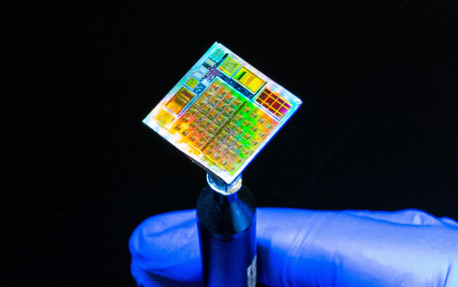
The world’s first fully integrated and functional microchip based on exotic two-dimensional materials has been fabricated at KAUST. The breakthrough demonstrates the potential of 2D materials to expand the functionality and performance of microchip-based technologies.
Since the first fabrication of atomically thin layers of graphite — called graphene — in 2004, there has been intense interest in such materials for advanced and novel applications due to their exotic and promising physical properties. But, despite two decades of research, functional microdevices based on these 2D materials have proved elusive due to the challenges in fabricating and handling such fragile thin films.
Inspired by recent achievements in Lanza’s lab on functional 2D films, the KAUST-led collaboration has now produced and demonstrated a prototype 2D-based microchip.
“Our motivation was to increase the technology readiness level of 2D material-based electronic devices and circuits by using conventional silicon-based CMOS microcircuits as a base and standard semiconductor fabrication techniques,” says Lanza. “The challenge, however, is that synthetic 2D materials can contain local defects such as atomic impurities that can cause small devices to fail. Also, it is very difficult to integrate the 2D material into the microchip without damaging it.”
Combining 2D Materials with CMOS
The research team optimized the design of the chip to make it easier to fabricate and minimize the effect of defects. They did this by fabricating standard complementary metal oxide semiconductor (CMOS) transistors on one side of the chip and feeding interconnects through to the underside, where the 2D material could be transferred reliably in small pads less than 0.25 micrometers across.
“We produced the 2D material — hexagonal boron nitride, or h-BN, on copper foil — and transferred it to the microchip using a low-temperature wet process, and we then formed electrodes over the top by conventional vacuum evaporation and photolithograpy, which are processes we have in-house,” says Lanza. “In this way we produced a 5×5 array of one-transistor/one-memristor cells connected in a crossbar matrix.”
Hexagonal Boron Nitride: The Ideal Memristor
The exotic properties of 2D h-BN, here just 18 atoms or 6 nanometers thick, make it an ideal “memristor” — a resistive component whose resistance can be set by the applied voltage. In this 5×5 arrangement, each of the microscale memristor pads is connected to a single dedicated transistor. This provides the fine voltage control needed to operate the memristor as a functional device with high performance and reliability over thousands of cycles, in this case as a low-power neural network element.
“With this flagship breakthrough, we are now talking with leading semiconducting companies to keep working in this direction,” Lanza says. “We are also considering installing our own wafer-scale industrial processing system for 2D materials at KAUST to advance this capability.”
Reference: “Hybrid 2D–CMOS microchips for memristive applications” by Kaichen Zhu, Sebastian Pazos, Fernando Aguirre, Yaqing Shen, Yue Yuan, Wenwen Zheng, Osamah Alharbi, Marco A. Villena, Bin Fang, Xinyi Li, Alessandro Milozzi, Matteo Farronato, Miguel Muñoz-Rojo, Tao Wang, Ren Li, Hossein Fariborzi, Juan B. Roldan, Guenther Benstetter, Xixiang Zhang, Husam N. Alshareef, Tibor Grasser, Huaqiang Wu, Daniele Ielmini and Mario Lanza, 27 March 2023, Nature.
DOI: 10.1038/s41586-023-05973-1
Never miss a breakthrough: Join the SciTechDaily newsletter.
Follow us on Google and Google News.
4 Comments
Amorphous distraction of tactile voltage recovery chips holds promising degree of regulation.
Wuhan-based Sino-Sux Labs made the announcement during a Ceramic Conference featuring Hunter Biden speaking on behalf of his ridiculous and mentally incompetent father.
“Loss of vertical stability in geriatric parcels has eviscerated the largest selection of candidates in the market,” Mr. Biden said.
Jeff Whacker of Peter Holdings is dealing with financial issues that may not make sense to most inebriated people, especially in light of the Bud Light debacle in recent months.
Peter Pepper picked a peck of Pickled Peckers. He believes these will offset the sales deficiency created by the Anheuser Busch capitalization drop the has resulted in fire sale type transactions to divest equine assets and transportative objects on the restrictive market.
Alternative solutions to the point that we need is just what AB has been doing electronically wi major AI derivative transforms remaining viable in low current applications.
The use of stretto- based constants has proven efficacious in the larger industry categories of business.
The Big Nook approach to power management has become one of the most powerful tools to provide an understanding of what makes this special opportunity produce repeatable results. This whole process house was designed to provide a terminated system for any pronouncement by any means that is acceptable within narrow conditions.
Great move by humanity
What in the hell is Podwod talking about? And what does tayo even mean? I swear, the STD comment section is next level.