The conventional light microscope, still standard equipment in laboratories, underlies the fundamental laws of optics. Thus, the resolution is limited by diffraction to the so-called ‘Abbe limit’ – structural features smaller than a minimum of 200 nm cannot be resolved by this kind of microscope.
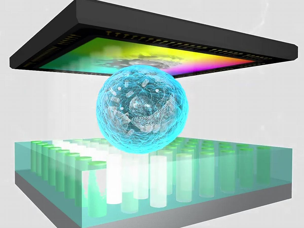
So far, all technologies for going beyond the Abbe limit rely on complex setups, with bulky components and advanced laboratory infrastructure. Even a conventional light microscope, in most configurations, is not suitable as a mobile gadget to do research out in the field or in remote areas. In the ChipScope project funded by the EU, a completely new strategy towards optical microscopy is explored. In classical optical microscopy, the analyzed sample area is illuminated simultaneously, collecting the light which is scattered from each point with an area-selective detector, e.g. the human eye or the sensor of a camera. In the ChipScope idea instead, a structured light source with tiny, individually addressable elements is utilized. As depicted in the figure, the specimen is located on top of this light source, in close vicinity. Whenever single emitters are activated, the light propagation depends on the spatial structure of the sample, very similar to what is known as shadow imaging in the macroscopic world. To obtain an image, the overall amount of light that is transmitted through the sample region is sensed by a detector, activating one light element at a time and thereby scanning across the sample space. If the light elements have sizes in the nanometer regime and the sample is in close contact to them, the optical near field is of relevance and super resolution imaging may become possible with a chip-based setup.
To realize this alternative idea, a bunch of innovative technology is required. The structured light source is realized by tiny light-emitting diodes (LEDs), which are developed at the University of Technology in Braunschweig, Germany. Due to their superior characteristics in comparison to other lighting systems, e.g. the classical light bulb or Halogen-based emitters, LEDs have conquered the market for general lighting applications in the past decades. However, to the present point, no structured LED arrays with individually addressable pixels down to the sub-µm regime are commercially available. This task belongs to the responsibility of TU Braunschweig within the frame of the ChipScope project. First LED arrays with pixel sizes down to 1 µm have already been demonstrated by the researchers, as depicted in the figure. They are based on gallium nitride (GaN), a semiconductor material that is commonly used for blue and white LEDs. Controlled structuring of such LEDs down to the sub-µm regime is extremely challenging. It is conducted by photo- and electron beam lithography, where structures in the semiconductor are defined with high precision by optical shadow masks or focused electron beams.
As a further component, highly sensitive light detectors are required for the microscope prototype. Here, Professor A. Dieguez’ group at the University of Barcelona develops so called single-photon avalanche detectors (SPADs) which can detect very low light intensities down to single photons. First tests with those detectors integrated into a prototype of the ChipScope microscope have already been conducted and have shown promising results. Moreover, a way to bring specimens into close vicinity of the structured light source is vital for proper microscope operation. An established technology to realize this utilizes microfluidic channels, where a fine system of channels is structured into a polymer matrix. Using high-precision pumps, a micro-volume liquid is driven through this system and carries the specimen along to the target position. This part of the microscope assembly is contributed by the Austrian Institute of Technology AIT. Further partners: Medical Univ. of Vienna, Univ. Tor Vergata Roma, LMU Munich and FSRM, Switzerland.
Never miss a breakthrough: Join the SciTechDaily newsletter.
Follow us on Google and Google News.