New research from the Max Planck Institute shows that silicon nanowires become doped with unexpectedly large amounts of aluminum during growth, increasing their conductivity and defying the laws of thermodynamics.
Nanoelectronics has taken another step forward. An international team including researchers from the Max Planck Institute of Microstructure Physics in Halle has discovered an effect that can be used to produce silicon nanowires with particularly attractive electrical and morphological properties. These nanowires are grown in an elegant way with aluminum as the catalyst. The scientists have now discovered that the silicon incorporates significantly more aluminum in the process than it is expected from known theories. This has beneficial effects on the properties of the wires, as the high proportion of aluminum – in semiconductor technology it is called the dopant – improves their conductivity. The effect could also be used to produce other highly-doped nanomaterials.
With completely pure silicon, a chip wouldn’t really work in the familiar way. Its conductivity is sufficient for current to flow in transistors only when the additional electrons or positive charges of impurity atoms increase the number of charge carriers in the semiconductor. This is why the semiconductor industry dopes silicon and other semiconductors, mixing a carefully measured quantity of impurity atoms into the materials. If the industry miniaturizes its components down to the nano-range in the future, it can possibly use an effect which a team of researchers from the Max Planck Institute of Microstructure Physics, the École Polytechnique in Montréal/Canada and Northwestern University in Illinois/USA has now discovered. In the method conventionally used to manufacture nanowires, the material is doped through a spontaneous incorporation of aluminum catalyst atoms.
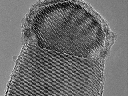
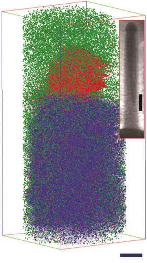
“The silicon here takes up as much as 10,000 times more aluminum than the laws of thermodynamics allow,” says Eckhard Pippel, one of the participating researchers from the Max Planck Institute of Microstructure Physics. Thermodynamics regulates, among other things, how much of a substance dissolves in another, and this applies to liquids and alloys of different metals alike. It states that fewer than one in a million atoms ought to be replaced by aluminum in a silicon crystal. However, the scientists determined that the aluminum content of the silicon wires is actually around four percent. And the aluminum atoms exhibit a completely uniform distribution in the material. The researchers made their discovery with the aid of ultraviolet laser-assisted atom probe tomography, which reveals the type and position of each individual atom in nanoscopic samples.
The nanowires cannot achieve the equilibrium chemical state
“On the day I saw the results, I jumped from the surprise,” says Oussama Moutanabbir, who carried out some of the investigations during his time at the Max Planck Institute of Microstructure Physics and is now a professor at the École Polytechnique in Montréal. “The data surprised us because of the high concentration, on the one hand, and also because the aluminum atoms do not form clusters in the silicon.” The aluminum content would be useless as a dopant if it were in the form of clusters, namely tiny accumulations of aluminum, as the number of charge carriers in silicon increases only when the aluminum atoms are distributed uniformly. This increase is important for electronic applications.
In order to control the unexpectedly strong embedding of aluminum and thus be in a position to use it for possible technical applications, the researchers looked for an explanation. “The fact that the concentration deviates so strongly from the predictions of thermodynamics is down to kinetic effects,” says Stephan Senz, one of the participating researchers from the Max Planck Institute of Microstructure Physics. Thermodynamics always describes an ideal state of equilibrium in nature in which chemical compounds strive to attain an energy content that is as low as possible and which they want to retain permanently. For crystals this means: they should preferably contain as few defects and impurity atoms as possible. When this ideal state is not achieved, the blame is always put on the kinetics, however. One of the processes which lead to the formation of a material then proceeds too quickly or too slowly for the ideal state of equilibrium to be achieved. This is precisely what happens during the formation of silicon nanowires.
Researchers grow nanowires from silicon by first distributing nano-particles of aluminum on a silicon surface. Aluminum melts at a lower temperature than silicon. And this is the crux of the matter. The researchers now place the silicon substrate sprinkled with aluminum islands into a chamber into which they allow silane, a very volatile silicon compound, to flow before heating the chamber to a temperature where only the aluminum melts, and not the silicon. Under these conditions, the silane converts into silicon and dissolves in the aluminum droplets.
A possible route to exotic chemical compounds
The drop does not stop embedding silicon as soon as it is saturated with silicon. Quite the opposite: it continues to incorporate silicon on its surface, but deposits it again onto the silicon surface below. The atoms arrange themselves row by row to form a silicon layer, similar to an inkjet printer printing a black surface line by line. As soon as one layer is finished under the drop, the next one forms. A nanowire thus gradually grows under each aluminum droplet.
In order to understand why more aluminum ends up in the silicon wire than is actually allowed, the researchers developed a model of how quickly the process proceeds on the atomic level. “The crucial aspect is the time available to the atoms to jump back and forth at the interface between the growing wire and the aluminum droplet” explains Oussama Moutanabbir. If this time is long, the atoms arrange themselves until the chemical equilibrium is achieved. However, the time is obviously not long enough for this. On the contrary, the time available for the atomic exchange stops as soon as one row of silicon atoms has been completed. “An aluminum atom that has previously been embedded remains permanently trapped,” says Moutanabbir. “Until now, it has been assumed that the atoms can be exchanged between metal drop and silicon until the whole silicon layer is complete.”
As the researchers have now clarified the process, it should be possible to apply it to the targeted doping of nanowires. “We suspect that the effect also occurs with other combinations of semiconductors and metals,” says Moutanabbir. “I also think it’s exciting that the growth of the nanowires occurs far away from the chemical equilibrium.” The researcher therefore hopes that similar processes can be used to produce nanomaterials with exotic chemical compositions, which are impossible to produce in the state of thermodynamic equilibrium.
Reference: “Colossal injection of catalyst atoms into silicon nanowires” by Oussama Moutanabbir, Dieter Isheim, Horst Blumtritt, Stephan Senz, Eckhard Pippel and David N. Seidman, 3 April 2013, Nature.
DOI: 10.1038/nature11999
Never miss a breakthrough: Join the SciTechDaily newsletter.
Follow us on Google and Google News.