Startup’s optoelectronic chips could reduce energy usage by up to 50 percent in data centers while increasing computing speeds.
With novel optoelectronic chips and a new partnership with a top silicon-chip manufacturer, MIT spinout Ayar Labs aims to increase speed and reduce energy consumption in computing, starting with data centers.
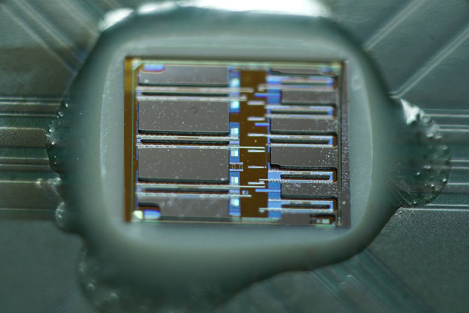
Backed by years of research at MIT and elsewhere, Ayar has developed chips that move data around with light but compute electronically. The unique design integrates speedy, efficient optical communications — with components that transmit data using light waves — into traditional computer chips, replacing less efficient copper wires.
According to the startup, the chips can reduce energy usage by about 95 percent in chip-to-chip communications and increase bandwidth tenfold over their copper-based counterparts. In massive data centers — Ayar’s first target application — run by tech giants such as Facebook and Amazon, the chips could cut total energy usage by 30 to 50 percent, says CEO Alex Wright-Gladstein MBA ’15.
“Right now there’s a bandwidth bottleneck in big data centers,” says Wright-Gladstein, who co-founded Ayar with Chen Sun Ph.D. ’15 and Mark Wade, a University of Colorado graduate and former MIT researcher. “That’s an exciting application and the first place that really needs this technology.”
In December, the startup penned a deal with GlobalFoundries, a top global silicon-chip manufacturer, to bring its first product, an optical input-output system called Brilliant, to market next year.
The chips could also be used in supercomputers, Wright-Gladstein adds, which have similar efficiency issues and speed constraints as data centers do. Down the road, the technology could also improve optics in various fields, from autonomous vehicles and medical devices to augmented reality. “We’re excited about not just what this can do for data centers, but what new things this will enable in the future,” Wright-Gladstein says.
Seeing the light
Ayar’s core technology — now backed by more than 25 academic papers — is a decade in the making. The research collaboration began in the mid-2000s at MIT as part of the Defense Advanced Research Project Agency’s Photonically Optimized Embedded Microprocessors (POEM) project, led by Vladimir Stojanovic, now an associate professor of electrical engineering and computer science at the University of California at Berkeley, in collaboration with Rajeev Ram, an MIT professor of electrical engineering and principal investigator for the Physical Optics and Electronics group, and Milos Popovic, now an assistant professor of electrical and computer engineering at Boston University.
The idea was to help data transmission keep up with Moore’s Law. The number of transistors on a chip may double every two years, Wright-Gladstein says, “but the amount of data we push across those copper pins hasn’t grown at the same rate.”
Computer chips send data between chips with different functions, such as logic chips and memory chips. With copper-based communications, however, the chips can’t send and receive enough data to take advantage of their increasing processing power. That’s caused a “bottleneck,” where chips must wait long durations to send and receive data. More than half the time in data centers, for instance, circuits are waiting for data to come and go, Wright-Gladstein says. “It’s a huge waste,” she says. “They’re using almost as much power idling as when they are working.”
One solution is light. An optical wire can transmit multiple data signals on different wavelengths of light, while copper wires are limited to one signal per wire. Optical chips can, therefore, transmit more information using significantly less space. Moreover, photonics produce very little waste heat. Data passing through copper wires generates large amounts of waste heat, which hurts efficiency in individual chips. This is an issue in data centers, where copper wires run inside and between servers.
At the time that the research groups of Ram, Stojanovic, and Popovic were working on the POEM project, large companies such as Intel and IBM were trying to design inexpensive, scalable optical chips. The collaboration — which then included Sun and Wade — took a different approach: They integrated optical components onto silicon chips, which are fabricated using the traditional CMOS semiconductor manufacturing process that churns out chips for pennies. “That was a radical idea at the time,” Wright-Gladstein says. “CMOS doesn’t lend itself well to optics, so industry veterans assumed you’d have to make major changes to get it to work.”
To avoid making changes to the CMOS process, the researchers focused on a new class of miniaturized optical components, including photodetectors, light modulators, waveguides, and optical filters that encode data on different wavelengths of light, and then transmit and decode it. They essentially “hacked” the traditional method for silicon chip design, using layers intended for electronics to build optical devices, and enabling chip designs to include optics more tightly configured than ever inside a chip’s structure.
In 2015, the researchers, together with Krste Asanovic’s team at UC Berkeley made the first processor to communicate using light and published the results in Nature. The chips, manufactured at a GlobalFoundries fabrication facility, contained 850 optical components and 70 million transistors, and performed as well as traditional chips manufactured at the same facility.
Taking the plunge
Behind the scenes, Wright-Gladstein was already thinking about commercialization. The year before the publication, she had enrolled in the MIT Sloan School of Management, specifically to meet researchers tackling clean energy. Taking 15.366 (Energy Ventures), which focuses on commercializing MIT clean technologies, she was chosen to select the technologies to bring into the classroom. “That was the perfect excuse to meet every researcher doing energy-related research,” Wright-Gladstein says.
From the vast pool of 300 labs, she came across Ram’s optoelectronic chips — which “blew me away,” she says. The energy industry was focused on equipment innovations to save energy in data centers. “But there wasn’t much focus on reducing energy through computing itself,” Wright-Gladstein says. “It seemed like a great way to make an impact.”
Wright-Gladstein formed a team in class to create a business plan and pitch deck. She also collaborated frequently with Sun and Wade in speaking with potential industry clients. When the MIT Clean Energy Prize rolled around, the three students entered the technology under the name, OptiBit — and won both grand prizes for $275,000, solidifying their decision to launch a startup.
“Having funds early on to pay ourselves low salaries and having a little cushion before raising venture capital funds really persuaded us all to take the plunge,” Wright-Gladstein says.
Setting up shop in San Francisco, the startup continued research and development, increasing the communication data rates of the technology. Last year, GlobalFoundries took interest in these constant innovations and struck a partnership with the startup, which included some undisclosed funding. This year, Ayar’s first prototypes should reach U.S. data centers, with a planned 2019 commercial release.
Solving the chip input-output problem is just the start. Ayar is also excited about what its new technology means for the field of optics, Wright-Gladstein says. Optical sensors, for instance, are used in self-driving or semiautonomous vehicles and expensive medical equipment. Lowering manufacturing costs, while increasing the computation power, of optoelectronic chips could make those technologies much less expensive and more accessible.
“We’re starting out solving this bottleneck problem in traditional silicon chips, but ultimately we’re excited about all the different places this technology will go,” Wright-Gladstein says. “This is going to change the availability of optics, and how the world can use optics, in ways beyond what we can predict right now.”
Never miss a breakthrough: Join the SciTechDaily newsletter.
Follow us on Google and Google News.