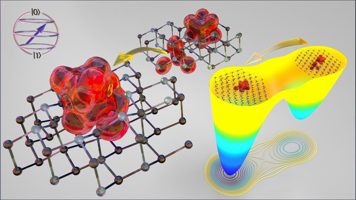
Simulation shows the pairing of silicon and carbon vacancies into a divacancy in silicon carbide. Red shows void volumes at defect sites. Upper left: qubit. Middle: divacancy formation in crystal lattice. Right: simulation results with combined MICCoM codes. Credit: University of Chicago
Team’s findings could help the design of industrially relevant quantum materials for sensing, computing, and communication.
“Vacancy” is a sign you want to see when searching for a hotel room on a road trip. When it comes to quantum materials, vacancies are also something you want to see. Scientists create them by removing atoms in crystalline materials. Such vacancies can serve as quantum bits or qubits, the basic unit of quantum technology.
Researchers at the U.S. Department of Energy’s (DOE) Argonne National Laboratory and the University of Chicago have made a breakthrough that should help pave the way for greatly improved control over the formation of vacancies in silicon carbide, a semiconductor.
Semiconductors are the material behind the brains in cell phones, computers, medical equipment, and more. For those applications, the existence of atomic-scale defects in the form of vacancies is undesirable, as they can interfere with performance. According to recent studies, however, certain types of vacancies in silicon carbide and other semiconductors show promise for the realization of qubits in quantum devices. Applications of qubits could include unhackable communication networks and hypersensitive sensors able to detect individual molecules or cells. Also possible in the future are new types of computers able to solve complex problems beyond the reach of classical computers.
“We are just at the beginning. We want to be able to do our computations much faster, simulate many more defects and determine what the best defects are for different applications.” — Giulia Galli, joint appointment with Argonne and the University of Chicago
“Scientists already know how to produce qubit-worthy vacancies in semiconductors such as silicon carbide and diamond,” said Giulia Galli, a senior scientist at Argonne’s Materials Science Division and professor of molecular engineering and chemistry at the University of Chicago. “But for practical new quantum applications, they still need to know much more about how to customize these vacancies with desired features.”
In silicon carbide semiconductors, single vacancies occur upon the removal of individual silicon and carbon atoms in the crystal lattice. Importantly, a carbon vacancy can pair with an adjacent silicon vacancy. This paired vacancy, called a divacancy, is a key candidate as a qubit in silicon carbide. The problem has been that the yield for converting single vacancies into divacancies has been low, a few percent. Scientists are racing to develop a pathway to increase that yield.
“To create actual defects in a sample, you shoot a beam of high-velocity electrons at it, and this knocks out individual atoms,” explained Elizabeth Lee, a postdoctoral researcher in the UChicago Pritzker School of Molecular Engineering. “But that electron bombardment also creates unwanted defects.”
Scientists can heal those defects by subsequently treating the sample at very high temperatures, above 1,300 degrees Fahrenheit, and cooling it down again to room temperature. The trick is to develop a process that will keep the wanted defects and heal the unwanted ones.
“By performing computer simulations at the atomic scale with high-performance computers, we can watch defects forming, moving, disappearing and rotating in a sample over time at different temperatures,” said Lee. “This is something that cannot be done experimentally, at present.”
Aided by a combination of sophisticated computational tools, the team’s simulations tracked the pairing of individual vacancies into a divacancy. Their efforts reaped a harvest of pivotal discoveries that should pave the way for new quantum devices. One is that the more silicon vacancies there are relative to carbon vacancies at the start of heat treatment, the more divacancies afterwards. Another is the determination of the best temperatures for creating stable divacancies and for altering their orientation within the crystal structure without destroying them.
Scientists may be able to use the latter discovery for aligning the orientation of all the divacancies in the same direction. That would be highly desirable for sensing applications able to operate with many times the resolution of today’s sensors.
Video shows divacancy changing its orientation. Credit: University of Chicago
“A totally unexpected and exciting finding was that divacancies can convert into an entirely new type of defect,” added Lee. These newly discovered defects consist of two carbon vacancies paired with what scientists call an anti-site. That is a site in which a carbon atom has filled the vacancy left open by the removal of a silicon atom.
A first of its kind, the team’s simulations were made possible by the development of new simulation algorithms and the coupling of computer codes developed by the DOE-funded Midwest Integrated Center for Computational Materials (MICCoM), headquartered at Argonne and led by Galli. Juan de Pablo a senior scientist in the Materials Science Division and UChicago professor of molecular engineering, developed the new algorithms, which are based on concepts from machine learning, a form of artificial intelligence.
“The formation and the motion of vacancies or defects in semiconductors are what we call rare events,” said de Pablo. “Such events happen on time scales much too long to study in conventional molecular simulations, even on the fastest computer on the planet. It is critical that we develop new ways of promoting the occurrence of these events without altering the underlying physics. That’s what our algorithms do; they make the impossible possible.”
Lee coupled the various codes, building on the work of MICCoM scientists Galli and de Pablo. Over the years, several other scientists were also involved in code coupling, including Francois Gygi at the University of California, Davis, and Jonathan Whitmer at Notre Dame University. The outcome is an important and powerful new toolset combining quantum theory and simulations for investigating vacancy formation and behavior. This will be applicable to not only silicon carbide, but other promising quantum materials.
“We are just at the beginning,” said Galli. “We want to be able to do our computations much faster, simulate many more defects, and determine what the best defects are for different applications.”
Reference: “Stability and molecular pathways to the formation of spin defects in silicon carbide” by Elizabeth M. Y. Lee, Alvin Yu, Juan J. de Pablo and Giulia Galli, 3 November 2021, Nature Communications.
DOI: 10.1038/s41467-021-26419-0
The team’s paper, “Stability and molecular pathways to the formation of spin defects in silicon carbide,” appeared in Nature Communications. Also contributing was postdoctoral fellow Alvin Yu, University of Chicago. This work was supported by the DOE Office of Basic Energy Sciences. The computationally intense simulations used several high-performance computing resources: Bebop in Argonne’s Laboratory Computing Resource Center; the Argonne Leadership Computing Facility (ALCF), a DOE Office of Science user facility; and the University of Chicago’s Research Computing Center. The team was awarded access to ALCF computing resources through DOE’s Innovative and Novel Computational Impact on Theory and Experiment, or INCITE, program.


Be the first to comment on "Quantum Breakthrough: How To Transform Vacancies Into Quantum Information"