
Researchers have developed a brain-inspired nanoelectronic device that could significantly reduce the energy demands of artificial intelligence systems.
Researchers have created a new type of nanoelectronic device that could significantly reduce the energy demands of artificial intelligence by taking inspiration from how the human brain works.
A team led by the University of Cambridge developed a modified form of hafnium oxide that functions as a highly stable, low-energy “memristor” — a component designed to replicate how neurons efficiently connect and communicate in the brain. The findings were published in Science Advances.
Today’s AI systems depend on traditional computer chips that constantly move data between memory and processing units. This ongoing data transfer consumes large amounts of electricity, and demand is rising quickly as AI becomes more widely used across industries.
Neuromorphic computing, which is modeled on the brain, offers a different approach. By combining data storage and processing in the same location, it could cut energy use by up to 70% while operating at very low power. Systems built this way could also adapt more easily, similar to how the brain learns over time.
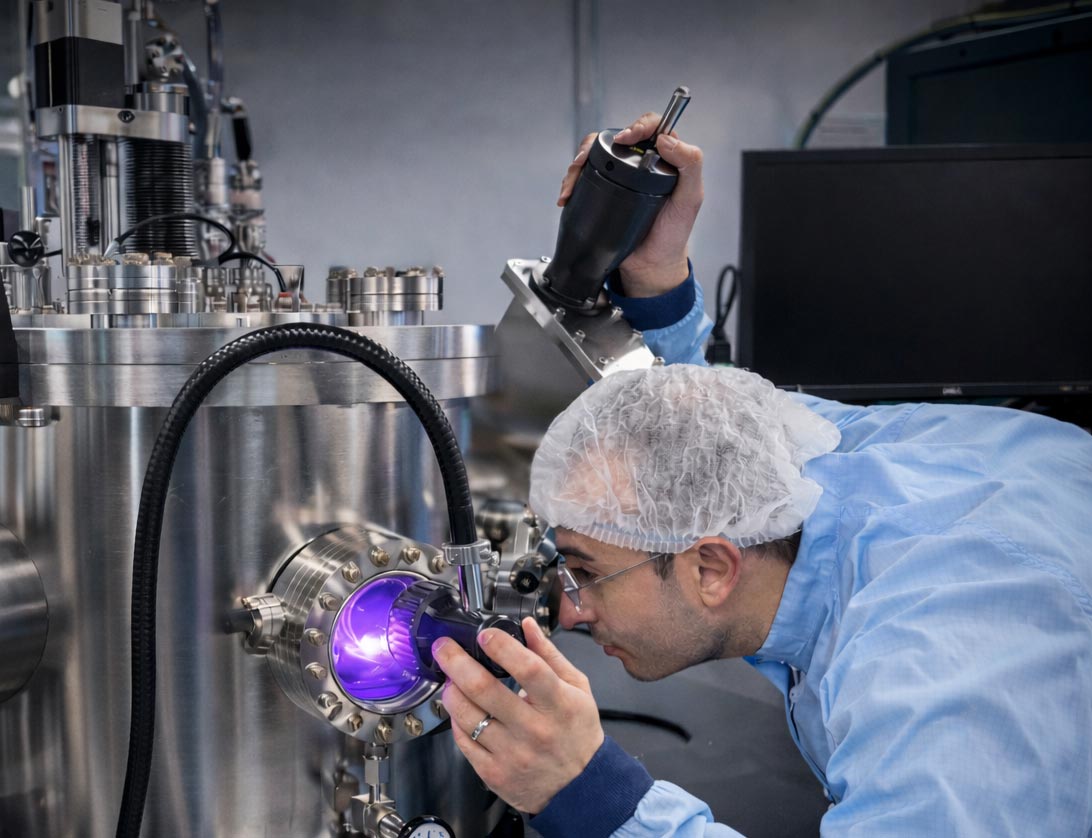
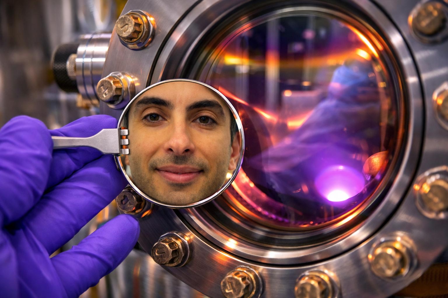
“Energy consumption is one of the key challenges in current AI hardware,” said lead author Dr. Babak Bakhit, from Cambridge’s Department of Materials Science and Metallurgy. “To address that, you need devices with extremely low currents, excellent stability, outstanding uniformity across switching cycles and devices, and the ability to switch between many distinct states.”
Moving Beyond Conventional Memristors
Most memristors today work by forming tiny conductive filaments inside metal oxide materials. These filaments can behave unpredictably and often require high voltages to operate, which limits their use in large-scale computing and data storage.
The Cambridge researchers took a different approach. They engineered a hafnium-based thin film that switches states without relying on filaments. By introducing strontium and titanium and using a two-step growth process, they created small electronic gates, or “p-n junctions,” within the oxide at the interface between layers.
This structure allows the device to adjust its resistance smoothly by changing the energy barrier at the interface, instead of forming or breaking filaments.
Bakhit, who is also affiliated with Cambridge’s Department of Engineering, said this design addresses a major limitation of existing memristors. “Filamentary devices suffer from random behaviour,” he said. “But because our devices switch at the interface, they show outstanding uniformity from cycle to cycle and from device to device.”
Performance and Learning Capabilities
The new devices achieved switching currents about one million times lower than some conventional oxide-based memristors. They also demonstrated hundreds of stable conductance levels, which are essential for analog “in-memory” computing.
In lab testing, the devices withstood tens of thousands of switching cycles and retained stored information for about a day. They also replicated key biological learning behaviors, including spike-timing dependent plasticity, where the strength of connections changes based on the timing of signals between neurons.
“These are the properties you need if you want hardware that can learn and adapt, rather than just store bits,” said Bakhit.
Remaining Challenges and Future Potential
There are still obstacles to address. The current manufacturing process requires temperatures of about 700°C (1,292°F), which exceeds standard semiconductor production limits. “This is currently the main challenge in our device fabrication process,” said Bakhit. “But we’re now working on ways to bring the temperature down to make it more compatible with standard industry processes.”
Despite this limitation, Bakhit believes the technology could eventually be integrated into chip-scale systems. “If we can reduce the temperature and put these devices onto a chip, it would be a major step forward,” he said.
He added that the breakthrough followed several years of trial and error. Progress came late last year when he modified the two-stage deposition process by introducing oxygen only after the first layer had formed.
“I spent almost three years on this,” he said. “There were a huge number of failures. But at the end of November, we saw the first really good results. It’s still early days of course, but if we can solve the temperature issue, this technology could be game-changing because the energy consumption is so much lower and at the same time, the device performance is highly promising.”
Reference: “HfO2-based memristive synapses with asymmetrically extended p-n heterointerfaces for highly energy-efficient neuromorphic hardware” by Babak Bakhit, Xiao Xie, Simon M. Fairclough, Atif Jan, Ingemar Persson, Giuliana Di Martino, Bonan Zhu, Caterina Ducati, Quanxi Jia, Bilge Yildiz, Andrew J. Flewitt and Judith L. MacManus-Driscoll, 20 March 2026, Science Advances.
DOI: 10.1126/sciadv.aec2324
The research was supported in part by the Swedish Research Council (VR), the Royal Academy of Engineering, the Royal Society, and UK Research and Innovation (UKRI). A patent
Never miss a breakthrough: Join the SciTechDaily newsletter.
Follow us on Google and Google News.