Scalable synthesis of transition metal chalcogenide nanowires for next-gen electronics.
Researchers from Tokyo Metropolitan University have discovered a way to make self-assembled nanowires of transition metal chalcogenides at scale using chemical vapor deposition. By changing the substrate where the wires form, they can tune how these wires are arranged, from aligned configurations of atomically thin sheets to random networks of bundles.
This paves the way to industrial deployment in next-gen industrial electronics, including energy harvesting, and transparent, efficient, even flexible devices.
Electronics is all about making things smaller. Smaller features on a chip, for example, means more computing power in the same amount of space and better efficiency, essential to feeding the increasingly heavy demands of a modern IT infrastructure powered by machine learning and artificial intelligence. And as devices get smaller, the same demands are made of the intricate wiring that ties everything together.
The ultimate goal would be a wire that is only an atom or two in thickness. Such nanowires would begin to leverage completely different physics as the electrons that travel through them behave more and more as if they live in a one-dimensional world, not a 3D one.
In fact, scientists already have materials like carbon nanotubes and transition metal chalcogenides (TMCs), mixtures of transition metals and group 16 elements which can self-assemble into atomic-scale nanowires. The trouble is making them long enough, and at scale. A way to mass produce nanowires would be a game changer.
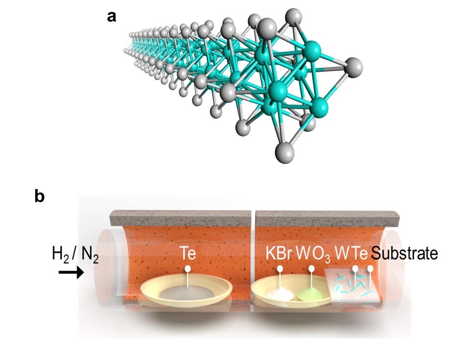
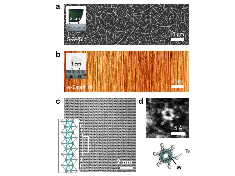
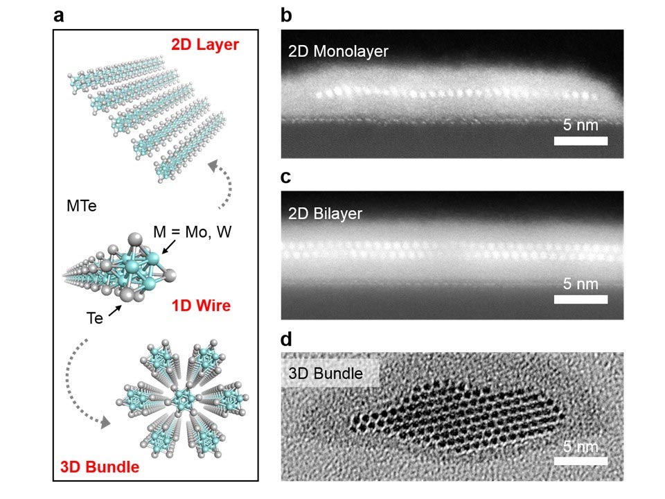
Now, a team led by Dr. Hong En Lim and Associate Professor Yasumitsu Miyata from Tokyo Metropolitan University has come up with a way of making long wires of transition metal telluride nanowires at unprecedentedly large scales. Using a process called chemical vapor deposition (CVD), they found that they could assemble TMC nanowires in different arrangements depending on the surface or substrate that they use as a template. Examples are shown in Figure 2; in (a), nanowires grown on a silicon/silica substrate form a random network of bundles; in (b), the wires assemble in a set direction on a sapphire substrate, following the structure of the underlying sapphire crystal. By simply changing where they are grown, the team now have access to centimeter-sized wafers covered in the arrangement they desired, including monolayers, bilayers and networks of bundles, all with different applications. They also found that the structure of the wires themselves were highly crystalline and ordered, and that their properties, including their excellent conductivity and 1D-like behavior, matched those found in theoretical predictions.
Having large amounts of long, highly crystalline nanowires is sure to help physicists characterize and study these exotic structures in more depth. Importantly, it’s an exciting step towards seeing real-world applications of atomically-thin wires, in transparent and flexible electronics, ultra-efficient devices and energy harvesting applications.
Reference: “Wafer-Scale Growth of One-Dimensional Transition-Metal Telluride Nanowires” by Hong En Lim, Yusuke Nakanishi, Zheng Liu, Jiang Pu, Mina Maruyama, Takahiko Endo, Chisato Ando, Hiroshi Shimizu, Kazuhiro Yanagi, Susumu Okada, Taishi Takenobu and Yasumitsu Miyata, 13 December 2020, Nano Letters.
DOI: 10.1021/acs.nanolett.0c03456
This work was supported by JST CREST Grants (JPMJCR16F3, JPMJCR17I5), Japan Society for the Promotion of Science (JSPS) KAKENHI Grants-in-Aid for Scientific Research (B) (JP18H01832, JP19H02543, JP20H02572, JP20H02573), Young Scientists (JP19K15383, JP19K15393), Scientific Research on Innovative Areas (JP20H05189, JP26102012), Specially Promoted Research (JP25000003), Challenging Research (Exploratory) (19K22127), and Scientific Research (A) (JP17H01069), and grants from the Murata Science Foundation (2019, H31-068) and the Japan Keirin Autorace Foundation (2020M-121). This work was partially conducted at the AIST Nano-Processing Facility supported by “Nanotechnology Platform Program” of the Ministry of Education, Culture, Sports, Science and Technology (MEXT), Japan. Grant Number JPMXP09F19008709 and 20009034.
Never miss a breakthrough: Join the SciTechDaily newsletter.
Follow us on Google and Google News.