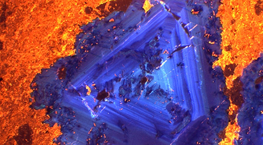
The phenomenon of cathodoluminescence gave geologists an easy way to identify quartz and other minerals in rock samples. Cathodoluminescence allows a piece of quartz to glow icy blue when put under an electron scanning microscope. Now, scientists have used this phenomenon to probe into nanostructures.
The scientists published their findings in the journal Physical Review Letters. The light, emitted after a beam of electrons kicks a material’s own electrons in to a higher-energy state, is faint and diffuse, thus discouraging scientists from harnessing it for fine-scale imaging. A Dutch group has found a way to collect and focus this light, which was previously ignored. They used it to probe a material’s nanoscale structure. The technology will reach the market early this year, giving scientists another tool to investigate the behavior of light in the interiors of the complex nanostructures used in lasers, light-based circuits and solar cells.
The technique has the advantage of combining optical and electron-based imaging. An electron beam can achieve a resolution of less than one nanometer, but a beam of light achieves a few hundred nanometers. Maps made by scattered or reflected electrons are not typically sensitive to the way light behaves in the sample. Cathodoluminescence can map the interaction of light and matter and since it’s triggered by a narrow beam of electrons, it can achieve the same nanoscale resolution.

The ultraprecise alignment of the sample is key to the functioning of the device, which includes a precisely shaped parabolic mirror that collects photons as they emerge from a sample bombarded with electrons. The photons are then sent through a system of lenses and a spectrometer to resolve the origin and energy of the light. The device is sensitive enough to pick up signals from materials that are barely luminescent, such as metals. Just as in an old-fashioned cathode-ray-tube color TV, the electron beam scans the sample to build up an image line by line.
The Dutch team has already used the technique to see how certain nanostructures interact with light. In a recent paper studying a layered construct of silver, glass, and silicon, they show that the phase velocity of visible light, the speed at which the peaks and troughs of the wave travel through the material, is as fast as if the light was traveling through vacuum. This is the explanation for the material’s overall refractive index of zero.
is effect had been predicted in layered structures called metamaterials; but in order to observe it, scientists required a higher-resolution map of light emissions than it was possible to produce until now. The team also mapped the distribution of light in the silicon nanodiscs used to coat solar cells to improve efficiency, as well as the small cavities of photonic crystals, components of chip-based lasers, and LEDs.
Reference: “Experimental Verification of n=0 Structures for Visible Light” by Ernst Jan R. Vesseur, Toon Coenen, Humeyra Caglayan, Nader Engheta and Albert Polman, 2 January 2013, Physical Review Letters.
DOI: 10.1103/PhysRevLett.110.013902
Never miss a breakthrough: Join the SciTechDaily newsletter.
Follow us on Google and Google News.