Engineers from MIT and the Masdar Institute of Science and Technology have developed a new solar cell that combines two different layers of sunlight-absorbing material to harvest a broader range of the sun’s energy.
The cost of solar power is beginning to reach price parity with cheaper fossil fuel-based electricity in many parts of the world, yet the clean energy source still accounts for just slightly more than 1 percent of the world’s electricity mix.
Solar, or photovoltaic (PV), cells, which convert sunlight into electrical energy, have a large role to play in boosting solar power generation globally, but researchers still face limitations to scaling up this technology. For example, developing very high-efficiency solar cells that can convert a significant amount of sunlight into usable electrical energy at very low costs remains a significant challenge.
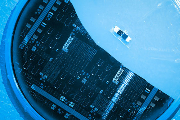
A team of researchers from MIT and the Masdar Institute of Science and Technology may have found a way around this seemingly intractable tradeoff between efficiency and cost. The team has developed a new solar cell that combines two different layers of sunlight-absorbing material to harvest a broader range of the sun’s energy. The researchers call the device a “step cell,” because the two layers are arranged in a stepwise fashion, with the lower layer jutting out beneath the upper layer, in order to expose both layers to incoming sunlight. Such layered, or “multijunction,” solar cells are typically expensive to manufacture, but the researchers also used a novel, low-cost manufacturing process for their step cell.
The team’s step-cell concept can reach theoretical efficiencies above 40 percent and estimated practical efficiencies of 35 percent, prompting the team’s principal investigators — Masdar Institute’s Ammar Nayfeh, associate professor of electrical engineering and computer science, and MIT’s Eugene Fitzgerald, the Merton C. Flemings-SMA Professor of Materials Science and Engineering — to plan a startup company to commercialize the promising solar cell.
Fitzgerald, who has launched several startups, including AmberWave Systems Corporation, Paradigm Research LLC, and 4Power LLC, thinks the step cells might be ready for the PV market within the next year or two.
The team presented its initial proof-of-concept step cell in June at the 43rd IEEE Photovoltaic Specialists Conference in Portland, Oregon. The researchers have also reported their findings at the 40th and 42nd annual conferences, and in the Journal of Applied Physics and IEEE Journal of Photovoltaics.
Beyond silicon
Traditional silicon crystalline solar cells, which have been touted as the industry’s gold standard in terms of efficiency for over a decade, are relatively cheap to manufacture, but they are not very efficient at converting sunlight into electricity. On average, solar panels made from silicon-based solar cells convert between 15 and 20 percent of the sun’s energy into usable electricity.
Silicon’s low sunlight-to-electrical energy efficiency is partially due to a property known as its bandgap, which prevents the semiconductor from efficiently converting higher-energy photons, such as those emitted by blue, green, and yellow light waves, into electrical energy. Instead, only the lower-energy photons, such as those emitted by the longer red light waves, are efficiently converted into electricity.
To harness more of the sun’s higher-energy photons, scientists have explored different semiconductor materials, such as gallium arsenide and gallium phosphide. While these semiconductors have reached higher efficiencies than silicon, the highest-efficiency solar cells have been made by layering different semiconductor materials on top of each other and fine-tuning them so that each can absorb a different slice of the electromagnetic spectrum.
These layered solar cells can reach theoretical efficiencies upward of 50 percent, but their very high manufacturing costs have relegated their use to niche applications, such as on satellites, where high costs are less important than low weight and high efficiency.
The Masdar Institute-MIT step cell, in contrast, can be manufactured at a fraction of the cost because a key component is fabricated on a substrate that can be reused. The device may thus help boost commercial applications of high-efficiency, multijunction solar cells at the industrial level.
Steps to success
The step cell is made by layering a gallium arsenide phosphide-based solar cell, consisting of a semiconductor material that absorbs and efficiently converts higher-energy photons, on a low-cost silicon solar cell.
The silicon layer is exposed, appearing like a bottom step. This intentional step design allows the top gallium arsenide phosphide (GaAsP) layer to absorb the high-energy photons (from blue, green, and yellow light) leaving the bottom silicon layer free to absorb lower-energy photons (from red light) not only transmitted through the top layers but also from the entire visible light spectrum.
“We realized that when the top gallium arsenide phosphide layer completely covered the bottom silicon layer, the lower-energy photons were absorbed by the silicon germanium — the substrate on which the gallium arsenide phosphide is grown — and thus the solar cell had a much lower efficiency,” explains Sabina Abdul Hadi, a Ph.D. student at Masdar Institute whose doctoral dissertation provided the foundational research for the step-cell. “By etching away the top layer and exposing some of the silicon layers, we were able to increase the efficiency considerably.”
Working under Nayfeh’s supervision, Abdul Hadi conducted simulations based on experimental results to determine the optimal levels and geometrical configuration of the GaAsP layer on silicon to yield the highest efficiencies. Her findings resulted in the team’s initial proof-of-concept solar cell. Abdul Hadi will continue supporting the step cell’s technological development as a post-doctoral researcher at Masdar Institute.
On the MIT side, the team developed the GaAsP, which they did by growing the semiconductor alloy on a substrate made of silicon germanium (SiGe).
“Gallium arsenide phosphide cannot be grown directly on silicon, because its crystal lattices differ considerably from silicon’s, so the silicon crystals become degraded. That’s why we grew the gallium arsenide phosphide on the silicon germanium — it provides a more stable base,” explains Nayfeh.
The problem with the silicon germanium under the GaAsP layer is that SiGe absorbs the lower-energy light waves before it reaches the bottom silicon layer, and SiGe does not convert these low-energy light waves into the current.
“To get around the optical problem posed by the silicon germanium, we developed the idea of the step cell, which allows us to leverage the different energy absorption bands of gallium arsenide phosphate and silicon,” says Nayfeh.
The step cell concept led to an improved cell in which the SiGe template is removed and re-used, creating a solar cell in which GaAsP cell tiles are directly on top of a silicon cell. The step-cell allows for SiGe reuse since the GaAsP cell tiles can be under-cut during the transfer process. Explaining the future low-cost fabrication process, Fitzgerald says: “We grew the gallium arsenide phosphide on top of the silicon germanium, patterned it in the optimized geometric configuration, and bonded it to a silicon cell. Then we etched through the patterned channels and lifted off the silicon germanium alloys on the silicon. What remains then, is a high-efficiency tandem solar cell and a silicon germanium template, ready to be reused.”
Because the tandem cell is bonded together, rather than created as a monolithic solar cell (where all layers are grown onto a single substrate), the SiGe can be removed and reused repeatedly, which significantly reduces the manufacturing costs.
“Adding that one layer of the gallium arsenide phosphide can really boost efficiency of the solar cell but because of the unique ability to etch away the silicon germanium and reuse it, the cost is kept low because you can amortize that silicon germanium cost over the course of manufacturing many cells,” Fitzgerald adds.
Filling a market gap
Fitzgerald believes the step cell fits well in the existing gap of the solar PV market, between the super high-efficiency and low-efficiency industrial applications. And as volume increases in this market gap, the manufacturing costs should be driven down even further over time.
This project began as one of nine Masdar Institute-MIT Flagship Research Projects, which are high-potential projects involving faculty and students from both universities. The MIT and Masdar Institute Cooperative Program helped launch the Masdar Institute in 2007. Research collaborations between the two institutes address global energy and sustainability issues, and seek to develop research and development capabilities in Abu Dhabi.
“This research project highlights the valuable role that research and international collaboration plays in developing a commercially relevant technology-based innovation, and it is a perfect demonstration of how a research idea can transform into an entrepreneurial reality,” says Nayfeh.
References:
“Theoretical efficiency limit for a two-terminal multi-junction “step-cell” using detailed balance method” by Sabina Abdul Hadi, Eugene A. Fitzgerald and Ammar Nayfeh, 19 February 2016, Journal of Applied Physics.
DOI: 10.1063/1.4942223
“Design Optimization of Single-Layer Antireflective Coating for GaAs1−xPx/Si Tandem Cells With x=0, 0.17, 0.29, and 0.37″ by Sabina Abdul Hadi, Tim Milakovich, Mayank T. Bulsara, Sueda Saylan, Marcus S. Dahlem, Eugene A. Fitzgerald and Ammar Nayfeh, 1 January 2015, IEEE Journal of Photovoltaics.
DOI: 10.1109/JPHOTOV.2014.2363559
Never miss a breakthrough: Join the SciTechDaily newsletter.
Follow us on Google and Google News.
8 Comments
I am going to buy this next year at Home Depot!
Can it produce power 24/7?
JOHN . DID YOU READ . IT CATCHES DIFFERENT WAVE LENGTH OF SUNLIGHT. YOU DON’T GET SUNLIGHT IN THE NIGHT ….. DUH !
The really sad part is an oil company WILL BUY the patent then let it die. You would be surprised how many inventions have been bought out and killed for the name of profit.
We studied this when I was in school. I got my BSEE degree in 1981
This is nothing new – we already use this technology on solar cells installed in extra terrestrial devices. I has been around since the 1980s and was initially developed by USSR scientists.
I’ve been reading about a solar electrical energy design which was apparently discovered in 2012. It’s promoted as “Backyard Revolution”. Can you tell me if this is true, or is it a scam?
Is amazing how certain folks belittle scientific developments especially when it’s just sprouting. These antics may or will easily dishearten even an enthusiastic researcher into culling what could evolve into a promising and magnificent development later on especially in the days of high speed communications. Something that could really take off with the possible & valuable contributions of minds and technology from all over eventually leading to fantastic developments.