Atomically thin materials are a promising alternative to silicon-based transistors; now researchers can connect them more efficiently to other chip elements.
Moore’s Law, the famous prediction that the number of transistors that can be packed onto a microchip will double every couple of years, has been bumping into basic physical limits. These limits could bring decades of progress to a halt, unless new approaches are found.
One new direction being explored is the use of atomically thin materials instead of silicon as the basis for new transistors, but connecting those “2D” materials to other conventional electronic components has proved difficult.
Now researchers at MIT, the University of California at Berkeley, the Taiwan Semiconductor Manufacturing Company, and elsewhere have found a new way of making those electrical connections, which could help to unleash the potential of 2D materials and further the miniaturization of components — possibly enough to extend Moore’s Law, at least for the near future, the researchers say.
The findings are described in the journal Nature, in a paper by recent MIT graduates Pin-Chun Shen PhD ’20 and Cong Su PhD ’20, postdoc Yuxuan Lin PhD ’19, MIT professors Jing Kong, Tomas Palacios, and Ju Li, and 17 others at MIT, UC Berkeley, and other institutions.

Bismuth Breakthrough in Contact Resistance
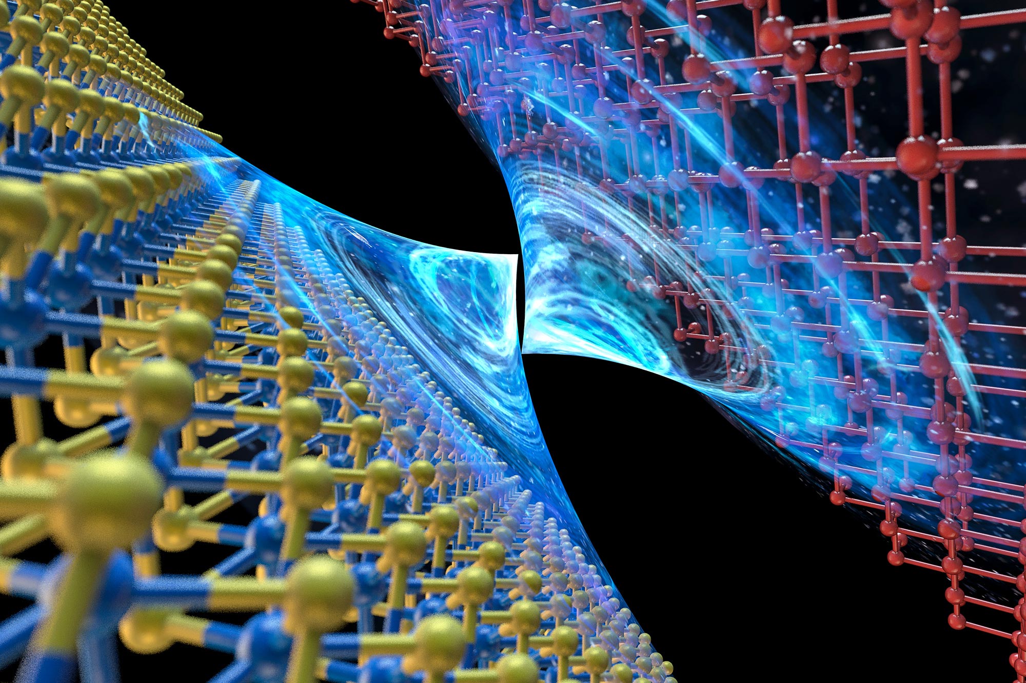
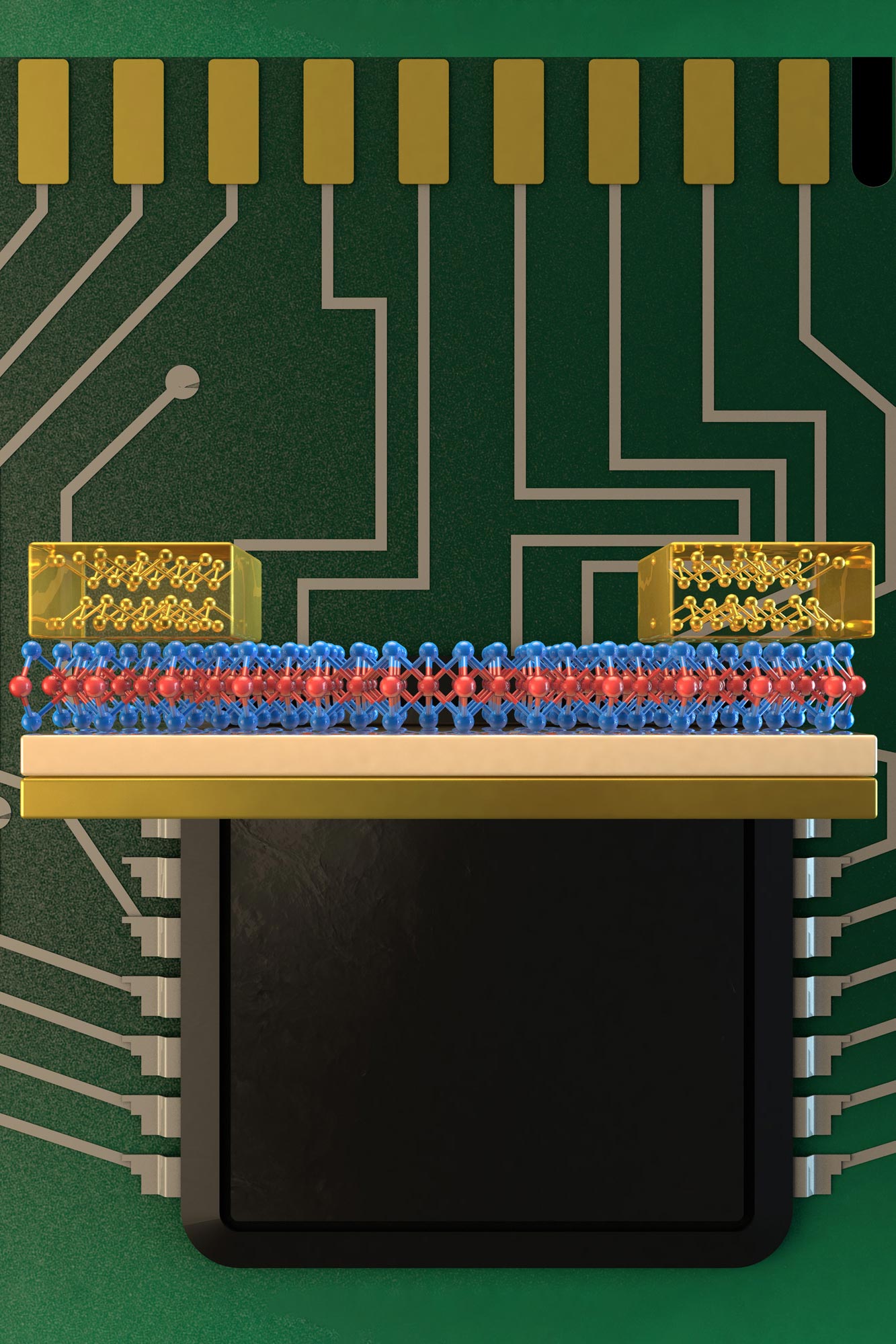
“We resolved one of the biggest problems in miniaturizing semiconductor devices, the contact resistance between a metal electrode and a monolayer semiconductor material,” says Su, who is now at UC Berkeley. The solution proved to be a simple one: the use of a semimetal, the element bismuth, to take the place of ordinary metals to connect with the monolayer material.
Such ultrathin monolayer materials, in this case molybdenum disulfide, are seen as a major contender for a way around the miniaturization limits now being encountered by silicon-based transistor technology. But creating an efficient, highly conductive interface between such materials and metal conductors, in order to connect them to each other and to other devices and power sources, was a challenge holding back progress toward such solutions, Su says.
The interface between metals and semiconductor materials (including these monolayer semiconductors) produces a phenomenon called metal-induced gap state, which leads to the formation of a Schottky barrier, a phenomenon that inhibits the flow of charge carriers. The use of a semimetal, whose electronic properties fall between those of metals and semiconductors, combined with proper energy alignment between the two materials, turned out to eliminate the problem.
New Hope for Transistor Miniaturization
Lin explains that the rapid pace of miniaturization of the transistors that make up computer processors and memory chips has stalled out before, around 2000, until a new development that allowed for a three-dimensional architecture of semiconductor devices on a chip broke the logjam in 2007 and rapid progress resumed. But now, he says, “we think we are on the edge of another bottleneck.”
Subnanometer Scale Devices
So-called two-dimensional materials, thin sheets just one or a few atoms thick, meet all the requirements for enabling a further leap in miniaturization of transistors, potentially reducing by several times a key parameter called the channel length — from around 5 to 10 nanometers, in current cutting-edge chips, to a subnanometer scale. A variety of such materials are being widely explored, including a whole family of compounds known as transition metal dichalcogenides. The molybdenum disulfide used in the new experiments belongs to this family.
The issue of achieving a low-resistance metal contact with such materials has also been hampering basic research on the physics of these novel monolayer materials. Because existing connection methods have such high resistance, the tiny signals needed to monitor the behavior of electrons in the material are too weak to get through. “There are numerous examples coming from the physics side that call for a low-contact resistance between the metal and a semiconductor. So, it’s a huge problem in the physics world as well,” Su says.
Figuring out how to scale up and integrate such systems at a commercial level could take some time and require further engineering. But for such physics applications, the researchers say, the impact of the new findings could be felt quickly. “I think in physics, many experiments can benefit from this technology immediately,” Su says.
Meanwhile, the researchers continue to explore further, continuing to reduce the size of their devices and looking for other pairings of materials that might enable better electrical contacts to the other type of charge carriers, known as holes. They solved the problem for the so-called N-type transistor, but if they can find a combination of channel and electrical contact material to enable an efficient monolayer P-type transistor as well, that would open up many new possibilities for next-generation chips, they say.
Reference: “Ultralow contact resistance between semimetal and monolayer semiconductors” by Pin-Chun Shen, Cong Su, Yuxuan Lin, Ang-Sheng Chou, Chao-Ching Cheng, Ji-Hoon Park, Ming-Hui Chiu, Ang-Yu Lu, Hao-Ling Tang, Mohammad Mahdi Tavakoli, Gregory Pitner, Xiang Ji, Zhengyang Cai, Nannan Mao, Jiangtao Wang, Vincent Tung, Ju Li, Jeffrey Bokor, Alex Zettl, Chih-I Wu, Tomás Palacios, Lain-Jong Li and Jing Kong, 12 May 2021, Nature.
DOI: 10.1038/s41586-021-03472-9
Besides MIT and the University of California at Berkeley, the team included researchers at Lawrence Berkeley National Laboratory, the Taiwan Semiconductor Manufacturing Company, the National Taiwan University, and King Abdullah University of Science and Technology in Saudi Arabia. The work was supported by the National Science Foundation, the U.S. Army Research Office, the Office of Naval research, and the U.S. Department of Energy.
Never miss a breakthrough: Join the SciTechDaily newsletter.
Follow us on Google and Google News.