Engineers mix and match materials to make new stretchy electronics: Next-generation devices made with new “peel and stack” method may include electronic chips worn on the skin.
At the heart of any electronic device is a cold, hard computer chip, covered in a miniature city of transistors and other semiconducting elements. Because computer chips are rigid, the electronic devices that they power, such as our smartphones, laptops, watches, and televisions, are similarly inflexible.
Now a process developed by MIT engineers may be the key to manufacturing flexible electronics with multiple functionalities in a cost-effective way.
The process is called “remote epitaxy” and involves growing thin films of semiconducting material on a large, thick wafer of the same material, which is covered in an intermediate layer of graphene. Once the researchers grow a semiconducting film, they can peel it away from the graphene-covered wafer and then reuse the wafer, which itself can be expensive depending on the type of material it’s made from. In this way, the team can copy and peel away any number of thin, flexible semiconducting films, using the same underlying wafer.
In a paper published today (February 5, 2020) in the journal Nature, the researchers demonstrate that they can use remote epitaxy to produce freestanding films of any functional material. More importantly, they can stack films made from these different materials, to produce flexible, multifunctional electronic devices.
The researchers expect that the process could be used to produce stretchy electronic films for a wide variety of uses, including virtual reality-enabled contact lenses, solar-powered skins that mold to the contours of your car, electronic fabrics that respond to the weather, and other flexible electronics that seemed until now to be the stuff of Marvel movies.
“You can use this technique to mix and match any semiconducting material to have new device functionality, in one flexible chip,” says Jeehwan Kim, an associate professor of mechanical engineering at MIT. “You can make electronics in any shape.”
Kim’s co-authors include Hyun S. Kum, Sungkyu Kim, Wei Kong, Kuan Qiao, Peng Chen, Jaewoo Shim, Sang-Hoon Bae, Chanyeol Choi, Luigi Ranno, Seungju Seo, Sangho Lee, Jackson Bauer, and Caroline Ross from MIT, along with collaborators from the University of Wisconsin at Madison, Cornell University, the University of Virginia, Penn State University, Sun Yat-Sen University, and the Korea Atomic Energy Research Institute.
Buying time
Kim and his colleagues reported their first results using remote epitaxy in 2017. Then, they were able to produce thin, flexible films of semiconducting material by first placing a layer of graphene on a thick, expensive wafer made from a combination of exotic metals. They flowed atoms of each metal over the graphene-covered wafer and found the atoms formed a film on top of the graphene, in the same crystal pattern as the underlying wafer. The graphene provided a nonstick surface from which the researchers could peel away the new film, leaving the graphene-covered wafer, which they could reuse.
In 2018, the team showed that they could use remote epitaxy to make semiconducting materials from metals in groups 3 and 5 of the periodic table, but not from group 4. The reason, they found, boiled down to polarity, or the respective charges between the atoms flowing over graphene and the atoms in the underlying wafer.
Since this realization, Kim and his colleagues have tried a number of increasingly exotic semiconducting combinations. As reported in this new paper, the team used remote epitaxy to make flexible semiconducting films from complex oxides — chemical compounds made from oxygen and at least two other elements. Complex oxides are known to have a wide range of electrical and magnetic properties, and some combinations can generate a current when physically stretched or exposed to a magnetic field.
Kim says the ability to manufacture flexible films of complex oxides could open the door to new energy-havesting devices, such as sheets or coverings that stretch in response to vibrations and produce electricity as a result. Until now, complex oxide materials have only been manufactured on rigid, millimeter-thick wafers, with limited flexibility and therefore limited energy-generating potential.
The researchers did have to tweak their process to make complex oxide films. They initially found that when they tried to make a complex oxide such as strontium titanate (a compound of strontium, titanium, and three oxygen atoms), the oxygen atoms that they flowed over the graphene tended to bind with the graphene’s carbon atoms, etching away bits of graphene instead of following the underlying wafer’s pattern and binding with strontium and titanium. As a surprisingly simple fix, the researchers added a second layer of graphene.
“We saw that by the time the first layer of graphene is etched off, oxide compounds have already formed, so elemental oxygen, once it forms these desired compounds, does not interact as heavily with graphene,” Kim explains. “So two layers of graphene buys some time for this compound to form.”
Peel and stack
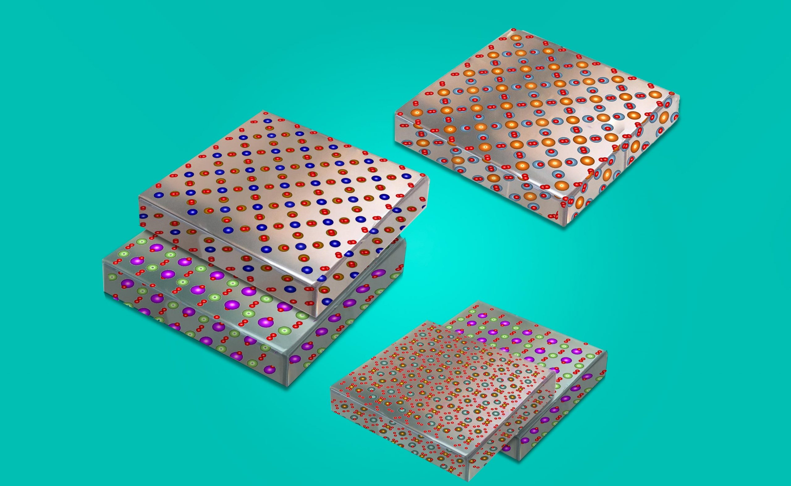
The team used their newly tweaked process to make films from multiple complex oxide materials, peeling off each 100-nanometer-thin layer as it was made. They were also able to stack together layers of different complex oxide materials and effectively glue them together by heating them slightly, producing a flexible, multifunctional device.
“This is the first demonstration of stacking multiple nanometers-thin membranes like LEGO blocks, which has been impossible because all functional electronic materials exist in a thick wafer form,” Kim says.
In one experiment, the team stacked together films of two different complex oxides: cobalt ferrite, known to expand in the presence of a magnetic field, and PMN-PT, a material that generates voltage when stretched. When the researchers exposed the multilayer film to a magnetic field, the two layers worked together to both expand and produce a small electric current.
The results demonstrate that remote epitaxy can be used to make flexible electronics from a combination of materials with different functionalities, which previously were difficult to combine into one device. In the case of cobalt ferrite and PMN-PT, each material has a different crystalline pattern. Kim says that traditional epitaxy techniques, which grow materials at high temperatures on one wafer, can only combine materials if their crystalline patterns match. He says that with remote epitaxy, researchers can make any number of different films, using different, reusable wafers, and then stack them together, regardless of their crystalline pattern.
“The big picture of this work is, you can combine totally different materials in one place together,” Kim says. “Now you can imagine a thin, flexible device made from layers that include a sensor, computing system, a battery, a solar cell, so you could have a flexible, self-powering, internet-of-things stacked chip.”
The team is exploring various combinations of semiconducting films and is working on developing prototype devices, such as something Kim is calling an “electronic tattoo” — a flexible, transparent chip that can attach and conform to a person’s body to sense and wirelessly relay vital signs such as temperature and pulse.
“We can now make thin, flexible, wearable electronics with the highest functionality,” Kim says. “Just peel off and stack up.”
Read Crystal-Stacking Process Opens Up “Nearly Limitless Possibilities” for New Materials for more on this breakthrough.
Reference: “Heterogeneous integration of single-crystalline complex-oxide membranes” by Hyun S. Kum, Hyungwoo Lee, Sungkyu Kim, Shane Lindemann, Wei Kong, Kuan Qiao, Peng Chen, Julian Irwin, June Hyuk Lee, Saien Xie, Shruti Subramanian, Jaewoo Shim, Sang-Hoon Bae, Chanyeol Choi, Luigi Ranno, Seungju Seo, Sangho Lee, Jackson Bauer, Huashan Li, Kyusang Lee, Joshua A. Robinson, Caroline A. Ross, Darrell G. Schlom, Mark S. Rzchowski, Chang-Beom Eom and Jeehwan Kim, 5 February 2020, Nature.
DOI: 10.1038/s41586-020-1939-z
This research was supported, in part, by the U.S. Defense Advanced Research Projects Agency.
Never miss a breakthrough: Join the SciTechDaily newsletter.
Follow us on Google and Google News.