
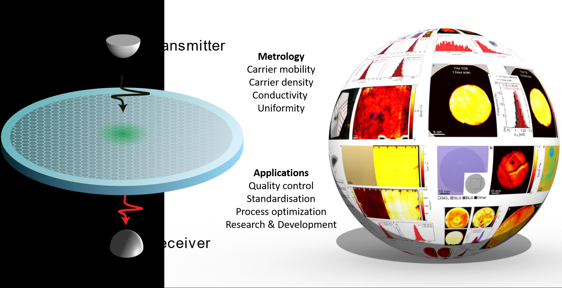
Graphene Flagship researchers have developed a new measurement standard for the analysis of graphene and layered materials that could accelerate production and optimize device fabrication.
X-ray scans revolutionized medical treatments by allowing us to see inside humans without surgery. Similarly, terahertz spectroscopy penetrates graphene films allowing scientists to make detailed maps of their electrical quality, without damaging or contaminating the material. The Graphene Flagship brought together researchers from academia and industry to develop and mature this analytical technique, and now a novel measurement tool for graphene characterization is ready.
The effort was possible thanks to the collaborative environment enabled by the Graphene Flagship European consortium, with participation by scientists from Graphene Flagship partners DTU, Denmark, IIT, Italy, Aalto University, Finland, AIXTRON, UK, IMEC, Belgium, Graphenea, Spain, Warsaw University, Poland, and Thales R&T, France, as well as collaborators in China, Korea, and the US.
Graphene is often ‘sandwiched’ between many different layers and materials to be used in electronic and photonic devices. This complicates the process of quality assessment. Terahertz spectroscopy makes things easier. It images the encapsulated materials and reveals the quality of the graphene underneath, exposing imperfections at critical points in the fabrication process. It is a fast, non-destructive technology that probes the electrical properties of graphene and layered materials, with no need for direct contact.
Terahertz Spectroscopy: Fast, Accurate, and Non-Destructive
The development of characterization techniques like terahertz spectroscopy is fundamental to accelerating large-scale production, as they guarantee that graphene-enabled devices are made consistently and predictably, without flaws. Quality control precedes trust. Thanks to other developments pioneered by the Graphene Flagship, such as roll-to-roll production of graphene and layered materials, fabrication technology is ready to take the next step. Terahertz spectroscopy allows us to ramp up graphene production without losing sight of the quality.
“This is the technique we needed to match the high-throughput production levels enabled by the Graphene Flagship,” explains Peter Bøggild from Graphene Flagship partner DTU. “We are confident that terahertz spectroscopy in graphene manufacturing will become as routine as X-ray scans in hospitals,” he adds. “In fact, thanks to terahertz spectroscopy you can easily map even meter-scale graphene samples without touching them, which is not possible with some other state-of-the-art techniques.” Furthermore, the Graphene Flagship is currently studying how to apply terahertz spectroscopy directly into roll-to-roll graphene production lines, and speed up the imaging.
Collaboration was key to this achievement. Graphene Flagship researchers in academic institutions worked closely with leading graphene manufacturers such as Graphene Flagship partners AIXTRON, Graphenea, and IMEC. “This is the best way to ensure that our solution is relevant to our end-users, companies that make graphene and layered materials on industrial scales,” says Bøggild. “Our publication is a comprehensive case study that highlights the versatility and reliability of terahertz spectroscopy for quality control and should guide our colleagues in applying the technique to many industrially relevant substrates such as silicon, sapphire, silicon carbide, and polymers,” he adds.
Setting standards is an important step for the development of any new material, to ensure it is safe, genuine and will offer a performance that is both reliable and consistent. That is why the Graphene Flagship has a dedicated work-group focused on the standardization of graphene, measurement and analytical techniques, and manufacturing processes. The newly developed method for terahertz spectroscopy is on track to become a standard technical specification, thanks to the work of the Graphene Flagship Standardisation Committee. “This will undoubtedly accelerate the uptake of this new technology, as it will outline how analysis and comparison of graphene samples can be done in a reproducible way,” explains Peter Jepsen from Graphene Flagship Partner DTU, who co-authors the study. “Terahertz spectroscopy is yet another step to increase the trust in graphene-enabled products,” he concludes.
Amaia Zurutuza, co-author of the paper and Scientific Director at Graphene Flagship partner Graphenea, says: “At Graphenea, we are convinced that terahertz imaging can enable the development of quality control techniques capable of matching manufacturing throughput requirements and providing relevant graphene quality information, which is essential in our path towards the successful industrialization of graphene.”
An Efficient, Scalable Mapping Tool for Industry
Thurid Gspann, the Chair of the Graphene Flagship Standardisation Committee, says: “This terahertz [spectroscopy] technique is expected to be widely adopted by industry. It does not require any particular sample preparation and is a mapping technique that allows one to analyze large areas in a time efficient way.”
Marco Romagnoli, Graphene Flagship Division Leader for Electronics and Photonics Integration, adds: “The terahertz spectroscopy tool for wafer-scale application is a state-of-the-art, high TRL system to characterize multilayer stacks on wafers that contain CVD graphene. It works in a short time and with good accuracy, and provides the main parameters of interest, such as carrier mobility, conductivity, scattering time and carrier density. This high-value technical achievement is also an example of the advantage of being part of a large collaborative project like the Graphene Flagship.”
Andrea C. Ferrari, Science and Technology Officer of the Graphene Flagship and Chair of its Management Panel, adds: “Yet again, Graphene Flagship researchers are pioneering a new characterization technique to facilitate the development of graphene technology. This helps us progress steadily on our innovation and technology roadmap and will benefit the industrial uptake of graphene in a wide range of applications.”
Reference: “Case studies of electrical characterisation of graphene by terahertz time-domain spectroscopy” by Patrick R Whelan, Binbin Zhou, Odile Bezencenet, Abhay Shivayogimath, Neeraj Mishra, Qian Shen, Bjarke S Jessen, Iwona Pasternak, David M A Mackenzie, Jie Ji, Cunzhi Sun, Pierre Seneor, Bruno Dlubak, Birong Luo, Frederik W Østerberg, Deping Huang, Haofei Shi, Da Luo, Meihui Wang, Rodney S Ruoff, Ben R Conran, Clifford McAleese, Cedric Huyghebaert, Steven Brems, Timothy J Booth, Ilargi Napal, Wlodek Strupinski, Dirch H Petersen, Stiven Forti, Camilla Coletti, Alexandre Jouvray, Kenneth B K Teo, Alba Centeno, Amaia Zurutuza, Pierre Legagneux, Peter U Jepsen and Peter Bøggild, 17 February 2021, 2D Materials.
DOI: 10.1088/2053-1583/abdbcb
Never miss a breakthrough: Join the SciTechDaily newsletter.
Follow us on Google and Google News.
1 Comment
Great. Now, what sort of images can terahertz technology produce of LIVING CELLS?
I would love a high definition movie of a cell dividing. Might learn something, too. Perhaps about the social lives of mitochondria…