By using an adhesive-like layer of nickel to peel graphene from silicon carbide, engineers at MIT have developed a technique to produce highly conductive wrinkle-free graphene wafers.
Graphene has been touted as a promising successor to silicon and for years researchers around the globe have observed that electrons can blitz through graphene at velocities approaching the speed of light. This is far faster than they can travel through silicon and other semiconducting materials and one of the reasons why scientists believe graphene has the potential to enable faster, more efficient electronic and photonic devices.
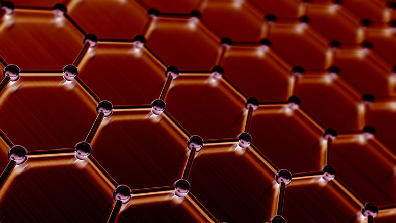
The holdup comes with the manufacturing process. It is extremely difficult to manufacture a single, perfectly flat, ultrathin sheet of carbon atoms, precisely aligned and linked together like chicken wire. Conventional fabrication processes often produce wrinkles, which can significantly limit graphene’s high-speed electrical performance.
Now a team of engineers from MIT think they might have solved this “wrinkle” problem. Using a technique that successfully produces wafer-scale, “single-domain” graphene (single layers of graphene that are uniform in both atomic arrangement and electronic performance), they have developed a new way to make graphene with fewer wrinkles and a way to iron out the wrinkles that do appear.
The researchers tested the electrical conductivity after fabricating and then flattening out the graphene, revealing that each wafer exhibited uniform performance; meaning that electrons flowed freely across each wafer, at similar speeds, even across previously wrinkled regions.
The new research is published today in the Proceedings of the National Academy of Sciences.
“For graphene to play as a main semiconductor material for industry, it has to be single-domain, so that if you make millions of devices on it, the performance of the devices is the same in any location,” says Jeehwan Kim, the Class of 1947 Career Development Assistant Professor in the departments of Mechanical Engineering and Materials Science and Engineering at MIT. “Now we can really produce single-domain graphene at wafer scale.”
Kim’s co-authors include Sanghoon Bae, Samuel Cruz, and Yunjo Kim from MIT, along with researchers from IBM, the University of California at Los Angeles, and Kyungpook National University in South Korea.
A patchwork of wrinkles
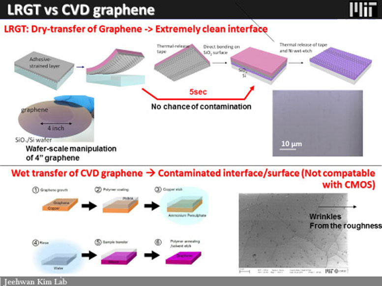
The most common way to make graphene involves chemical vapor deposition, or CVD, a process in which carbon atoms are deposited onto a crystalline substrate such as copper foil. Once the copper foil is evenly coated with a single layer of carbon atoms, scientists submerge the entire thing in acid to etch away the copper. What remains is a single sheet of graphene, which researchers then pull out from the acid.
The CVD process can produce relatively large, macroscropic wrinkles in graphene, due to the roughness of the underlying copper itself and the process of pulling the graphene out from the acid. The alignment of carbon atoms is not uniform across the graphene, creating a “polycrystalline” state in which graphene resembles an uneven, patchwork terrain, preventing electrons from flowing at uniform rates.
In 2013, while working at IBM, Kim and his colleagues developed a method to fabricate wafers of single-crystalline graphene, in which the orientation of carbon atoms is exactly the same throughout a wafer.
Rather than using CVD, his team produced single-crystalline graphene from a silicon carbide wafer with an atomically smooth surface, albeit with tiny, step-like wrinkles on the order of several nanometers. They then used a thin sheet of nickel to peel off the topmost graphene from the silicon carbide wafer, in a process called layer-resolved graphene transfer.
Ironing charges
In the newly published study, Kim and his colleagues discovered that the layer-resolved graphene transfer irons out the steps and tiny wrinkles in silicon carbide-fabricated graphene. Before transferring the layer of graphene onto a silicon wafer, the team oxidized the silicon, creating a layer of silicon dioxide that naturally exhibits electrostatic charges. When the researchers then deposited the graphene, the silicon dioxide effectively pulled graphene’s carbon atoms down onto the wafer, flattening out its steps and wrinkles.
Kim says this ironing method would not work on CVD-fabricated graphene, as the wrinkles generated through CVD are much larger, on the order of several microns.
“The CVD process creates wrinkles that are too high to be ironed out,” Kim notes. “For silicon carbide graphene, the wrinkles are just a few nanometers high, short enough to be flattened out.”
The researchers fabricated tiny transistors on multiple sites on each wafer, including across previously wrinkled regions, to test whether the flattened, single-crystalline graphene wafers were single-domain.
“We measured electron mobility throughout the wafers, and their performance was comparable,” Kim says. “What’s more, this mobility in ironed graphene is two times faster. So now we really have single-domain graphene, and its electrical quality is much higher [than graphene-attached silicon carbide].”
Kim says that while there are still challenges to adapting graphene for use in electronics, the group’s results give researchers a blueprint for how to reliably manufacture pristine, single-domain, wrinkle-free graphene at wafer scale.
“If you want to make any electronic device using graphene, you need to work with single-domain graphene,” Kim says. “There’s still a long way to go to make an operational transistor out of graphene. But we can now show the community guidelines for how you can make single-crystalline, single-domain graphene.”
Reference: “Unveiling the carrier transport mechanism in epitaxial graphene for forming wafer‐scale, single‐domain graphene” by Sang-Hoon Bae, Xiaodong Zhou, Seyoung Kim, Yun Seog Lee, Samuel S. Cruz, Yunjo Kim, James B. Hannon, Yang Yang, Devendra K. Sadana, Frances M. Ross, Hongsik Park and Jeehwan Kim, 3 April 2017, PNAS.
DOI: 10.1073/pnas.1620176114
Never miss a breakthrough: Join the SciTechDaily newsletter.
Follow us on Google and Google News.