Researchers at the University of Pennsylvania are pushing circuitry forward by replacing electricity with light. By moving to shorter wavelengths in the electromagnetic spectrum, they believed they could make things smaller, faster, and more efficient and have created the first physical demonstration of “lumped” optical circuit elements.
The technological world of the 21st century owes a tremendous amount to advances in electrical engineering, specifically, the ability to finely control the flow of electrical charges using increasingly small and complicated circuits. And while those electrical advances continue to race ahead, researchers at the University of Pennsylvania are pushing circuitry forward in a different way, by replacing electricity with light.
“Looking at the success of electronics over the last century, I have always wondered why we should be limited to electric current in making circuits,” said Nader Engheta, professor in the electrical and systems engineering department of Penn’s School of Engineering and Applied Science. “If we moved to shorter wavelengths in the electromagnetic spectrum — like light — we could make things smaller, faster, and more efficient.”

Different arrangements and combinations of electronic circuits have different functions, ranging from simple light switches to complex supercomputers. These circuits are in turn built of different arrangements of circuit elements, like resistors, inductors and capacitors, which manipulate the flow of electrons in a circuit in mathematically precise ways. And because both electric circuits and optics follow Maxwell’s equations — the fundamental formulas that describe the behavior of electromagnetic fields — Engheta’s dream of building circuits with light wasn’t just the stuff of imagination. In 2005, he and his students published a theoretical paper outlining how optical circuit elements could work.

Now, he and his group at Penn have made this dream a reality, creating the first physical demonstration of “lumped” optical circuit elements. This represents a milestone in a nascent field of science and engineering Engheta has dubbed “metatronics.”
Engheta’s research, which was conducted with members of his group in the electrical and systems engineering department, Yong Sun, Brian Edwards, and Andrea Alù, was published in the journal Nature Materials.
In electronics, the “lumped” designation refers to elements that can be treated as a black box, something that turns a given input to a perfectly predictable output without an engineer having to worry about what exactly is going on inside the element every time he or she is designing a circuit.
“Optics has always had its own analogs of elements, things like lenses, waveguides, and gratings,” Engheta said, “but they were never lumped. Those elements are all much larger than the wavelength of light because that’s all that could be easily built in the old days. For electronics, the lumped circuit elements were always much smaller than the wavelength of operation, which is in the radio or microwave frequency range.”
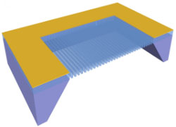
Nanotechnology has now opened that possibility for lumped optical circuit elements, allowing construction of structures that have dimensions measured in nanometers. In this experiment’s case, the structure was comb-like arrays of rectangular nanorods made of silicon nitrite.
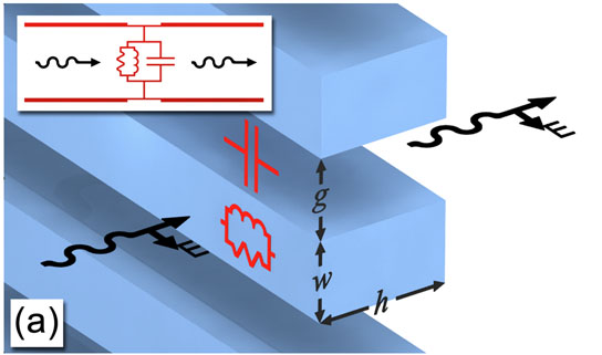
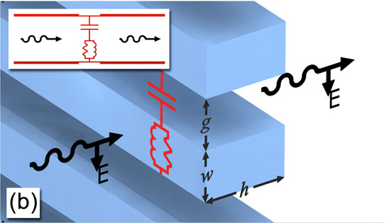
The “meta” in “metatronics” refers to metamaterials, the relatively new field of research where nanoscale patterns and structures embedded in materials allow them to manipulate waves in ways that were previously impossible. Here, the cross-sections of the nanorods and the gaps between them form a pattern that replicates the function of resistors, inductors and capacitors, three of the most basic circuit elements, but in optical wavelengths.
“If we have the optical version of those lumped elements in our repertoire, we can actually make designs similar to what we do in electronics but now for operation with light,” Engheta said. “We can build a circuit with light.”
In their experiment, the researchers illuminated the nanorods with an optical signal, a wave of light in the mid-infrared range. They then used spectroscopy to measure the wave as it passed through the comb. Repeating the experiment using nanorods with nine different combinations of widths and heights, the researchers showed that the optical “current” and optical “voltage” were altered by the optical resistors, inductors, and capacitors with parameters corresponding to those differences in size.
“A section of the nanorod acts as both an inductor and resistor, and the air gap acts as a capacitor,” Engheta said.
Beyond changing the dimensions and the material the nanorods are made of, the function of these optical circuits can be altered by changing the orientation of the light, giving metatronic circuits access to configurations that would be impossible in traditional electronics.
This is because a light wave has polarizations; the electric field that oscillates in the wave has a definable orientation in space. In metatronics, it is that electric field that interacts and is changed by elements, so changing the field’s orientation can be like rewiring an electric circuit.
When the plane of the field is in line with the nanorods, as in Figure A, the circuit is wired in parallel and the current passes through the elements simultaneously. When the plane of the electric field crosses both the nanorods and the gaps, as in Figure B, the circuit is wired in series and the current passes through the elements sequentially.
“The orientation gives us two different circuits, which is why we call this ‘stereo-circuitry,’” Engheta said. “We could even have the wave hit the rods obliquely and get something we don’t have in regular electronics: a circuit that’s neither in series or in parallel but a mixture of the two.”
This principle could be taken to an even higher level of complexity by building nanorod arrays in three dimensions. An optical signal hitting such a structure’s top would encounter a different circuit than a signal hitting its side. Building off their success with basic optical elements, Engheta and his group are laying the foundation for this kind of complex metatronics.
“Another reason for success in electronics has to do with its modularity,” he said. “We can make an infinite number of circuits depending on how we arrange different circuit elements, just like we can arrange the alphabet into different words, sentence,s and paragraphs.
“We’re now working on designs for more complicated optical elements,” Engheta said. “We’re on a quest to build these new letters one by one.”
Reference: “Experimental realization of optical lumped nanocircuits at infrared wavelengths” by Yong Sun, Brian Edwards, Andrea Alù and Nader Engheta, 29 January 2012, Nature Materials.
DOI: 10.1038/nmat3230
This work was supported in part by the U.S. Air Force Office of Scientific Research.
Andrea Alù is now an assistant professor at the University of Texas at Austin.
Never miss a breakthrough: Join the SciTechDaily newsletter.
Follow us on Google and Google News.