
This major scientific advance has implications for many fields, including energy-efficient computers and quantum technology.
Until recently, physicists widely believed that it was impossible to compress light below the so-called diffraction limit, except when utilizing metal nanoparticles, which also absorb light. As a result, it seemed to be impossible to compress light strongly in dielectric materials like silicon, which are essential for information technologies and had the significant advantage of not absorbing light. Interestingly, it was theoretically shown that the diffraction limit does not apply to dielectrics back in 2006. However, no one has been able to demonstrate this in the actual world due to the fact that it requires such complex nanotechnology that no one has yet been able to create the required dielectric nanostructures.
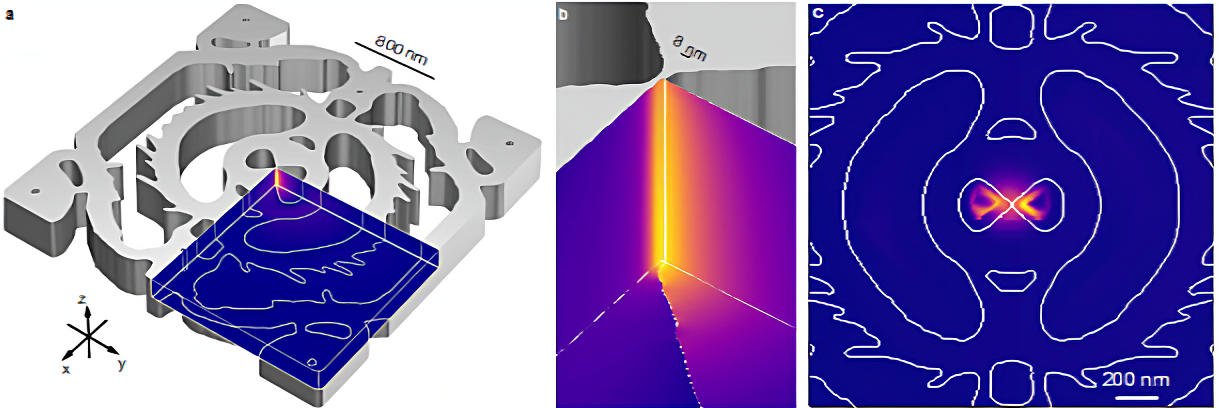
A research team from the Technical University of Denmark (DTU) has created a device known as a “dielectric nanocavity” that successfully concentrates light in a volume 12 times smaller than the diffraction limit. The finding is groundbreaking in optical research and was recently published in the journal Nature Communications.
“Although computer calculations show that you can concentrate light at an infinitely small point, this only applies in theory. The actual results are limited by how small details can be made, for example, on a microchip,” says Marcus Albrechtsen, Ph.D.-student at DTU Electro and the first author of the new article.
“We programmed our knowledge of real photonic nanotechnology and its current limitations into a computer. Then we asked the computer to find a pattern that collects the photons in an unprecedentedly small area – in an optical nanocavity – which we were also able to build in the laboratory.”
Optical nanocavities are structures that have been specially designed to retain light so that it does not travel normally but is tossed back and forth as if two mirrors were facing each other. The closer the mirrors are to one other, the more intense the light between them gets. For this experiment, the researchers created a bowtie structure, which is particularly effective in squeezing photons together due to its unique shape.
The Diffraction Limit
The theory of the diffraction limit describes that light cannot be focused to a volume smaller than half the wavelength in an optical system – for example, this applies to the resolution in microscopes.
However, nanostructures can consist of elements much smaller than the wavelength, which means that the diffraction limit is no longer a fundamental limit. Bowtie structures, in particular, can compress the light into very small volumes limited by the sizes of the bowtie and, thus, the quality of the nanofabrication.
When the light is compressed, it becomes more intense, enhancing interactions between light and materials such as atoms, molecules, and 2D materials.
Dielectric Materials
Dielectric materials are electrically insulating. Glass, rubber, and plastic are examples of dielectric materials, and they contrast with metals, which are electrically conductive.
An example of a dielectric material is silicon, which is often used in electronics but also in photonics.
Interdisciplinary Efforts and Excellent Methods
The nanocavity is made of silicon, the dielectric material on which most advanced modern technology is based. The material for the nanocavity was developed in cleanroom laboratories at DTU, and the patterns on which the cavity is based are optimized and designed using a unique method for topology optimization developed at DTU. Initially developed to design bridges and aircraft wings, it is now also used for nanophotonic structures.
“It required a great joint effort to achieve this breakthrough. It has only been possible because we have managed to combine world-leading research from several research groups at DTU,” says associate professor Søren Stobbe, who has led the research work.”
Important Breakthrough for Energy-Efficient Technology
The discovery could be decisive for developing revolutionary new technologies that may reduce the amount of energy-guzzling components in data centers, computers, telephones, etc.
The energy consumption for computers and data centers continues to grow, and there is a need for more sustainable chip architectures that use less energy. This can be achieved by replacing electrical circuits with optical components. The researchers’ vision is to use the same division of labor between light and electrons used for the Internet, where light is used for communication and electronics for data processing. The only difference is that both functionalities must be built into the same chip, which requires that the light be compressed to the same size as the electronic components. The breakthrough at DTU shows that it is, in fact, possible.
“There is no doubt that this is an important step to developing a more energy-efficient technology for, e.g., nanolasers for optical connections in data centers and future computers – but there is still a long way to go,” says Marcus Albrechtsen.
The researchers will now work further and refine methods and materials to find the optimal solution.
“Now that we have the theory and method in place, we will be able to make increasingly intense photons as the surrounding technology develops. I am convinced that this is just the first of a long series of major developments in physics and photonic nanotechnology centered around these principles,” says Søren Stobbe, who recently received the prestigious Consolidator Grant from the European Research Council of € 2 million for the development of a completely new type of light source based on the new cavities.
Reference: “Nanometer-scale photon confinement in topology-optimized dielectric cavities” by Marcus Albrechtsen, Babak Vosoughi Lahijani, Rasmus Ellebæk Christiansen, Vy Thi Hoang Nguyen, Laura Nevenka Casses, Søren Engelberth Hansen, Nicolas Stenger, Ole Sigmund, Henri Jansen, Jesper Mørk and Søren Stobbe, 21 October 2022, Nature Communications.
DOI: 10.1038/s41467-022-33874-w
The study was funded by the Villum Foundation Young Investigator Program, the Villum Foundation Experiment Program, the Danish National Research Foundation, the Independent Research Fund Denmark, and the Innovation Fund Denmark.
Never miss a breakthrough: Join the SciTechDaily newsletter.
Follow us on Google and Google News.
4 Comments
“Any sufficiently advanced technology is indistinguishable from magic.”
This gadget even *looks* like some sort of talisman.
Ive never seen anything like this before
Interesting stuff that is… Good job and more of the success from heart I wish!
Little hint I will give for friends of truth.. can reveal big mystery, but must find the key yourself:
– Not in the space photons can be seen, in space photons quickly redeem!
– Space is tiny as quant can be,
Compression limits also, you see!
– Follow the breadcrumbs and combine with the clue,
That with missing 1/2 in Alberts formula have something to do!
Good luck!
I am wondering if you have ever seen this? My late father ( Dr. Gerald C. Huth ) patented this several years ago but passed away before it was going to be developed.
See: https://patents.google.com/patent/US5689603A/en