Researchers in Finland have experimentally realized a long-predicted class of quantum material: a two-dimensional topological crystalline insulator.
Physicists at the University of Jyväskylä and Aalto University (Finland) have successfully created a two-dimensional topological crystalline insulator in the laboratory. This unusual quantum material was predicted by theory more than ten years ago, but producing it experimentally proved difficult because of challenges in preparing suitable materials.
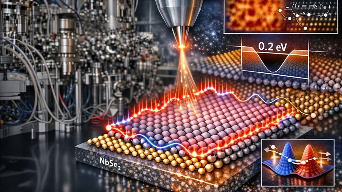
The research team achieved the long-awaited result in a study led by Associate Professor Kezilbeiek Shawulienu. The project involved collaboration with scientists at Aalto University, including Professor Peter Liljeroth and Professor Jose Lado. To build the material, the researchers deposited an atomically thin film of tin telluride (SnTe) consisting of two layers onto a niobium diselenide (NbSe2) substrate.
The scientists then examined the material’s electronic behavior using molecular beam epitaxy and low-temperature scanning tunneling microscopy. These techniques allowed them to analyze the structure with atomic-level precision. Within this two-dimensional system, they detected pairs of conducting states that appear along the edges of the material. These edge states are a defining feature of topological crystalline insulators and remain stable because they are protected by the symmetry of the crystal lattice.

Strain as a key to controlling topological edge states
The conducting edge states appear inside a wide electronic band gap that exceeds 0.2 eV. Measurements show that the SnTe film experiences compressive strain caused by the underlying substrate. This strain plays an essential role in stabilizing the topological phase of the material.
The experiments also demonstrate that these edge states respond to changes in strain. This means that adjusting the strain in the material could provide a way to control its electronic behavior.
Toward nanoscale devices
First principles quantum mechanical calculations support the experimental findings and confirm that the observed edge states arise from the material’s topological properties. The researchers also studied how nearby edge states interact with one another. Their measurements revealed energy shifts caused by both electrostatic effects and quantum tunneling.
Because the band gap is relatively large, the topological behavior of the material is expected to remain stable even at room temperature.
This newly realized system provides researchers with a powerful experimental platform for investigating two-dimensional topological states that can be tuned by strain. It may also contribute to the development of spin-based electronics and other nanoscale technologies in the future.
Reference: “Strain-induced two-dimensional topological crystalline insulator in bilayer SnTe” by Liwei Jing, Mohammad Amini, Adolfo O. Fumega, Orlando J. Silveira, Jose L. Lado, Peter Liljeroth and Shawulienu Kezilebieke, 21 January 2026, Nature Communications.
DOI: 10.1038/s41467-025-67520-y
Never miss a breakthrough: Join the SciTechDaily newsletter.
Follow us on Google and Google News.
2 Comments
Physicists should think deeply:
1. Is the two-dimensional in mathematics the same as the two-dimensional in physics?
2. Why is physics inseparable from mathematics?
3. Can physics be fundamentally separated from mathematics?
thanks for this