
Scientists are exploring 2D materials — sheets just one atom thick — with unique and promising electronic properties.
When two of these sheets are layered at specific angles, they can exhibit remarkable behaviors, such as superconductivity. Antonija Grubišić-Čabo, a materials scientist at the University of Groningen, and her colleagues investigated one such “twisted” material and found that it behaved in ways that defied existing theoretical predictions.
2D Materials and Superconductivity
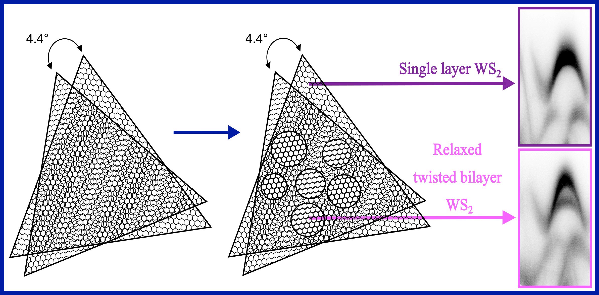
Grubišić-Čabo, along with collaborators from Poland, Germany, France, and Italy, studied sheets of a 2D material called tungsten disulfide. Theoretical predictions suggested that when two sheets, or a bilayer, are stacked at a precise angle of 4.4 degrees, the electrons within the material should exhibit collective behavior.
“And when they are so closely connected, their collective behavior can create new, fascinating effects,” explains Giovanna Feraco, first author of the study.
Unexpected Results in Electron Behavior
However, experiments did not reveal this predicted behavior. This discrepancy is linked to the interactions between atoms in the bilayer, which the twist is supposed to enhance.
“But by studying the electronic structure in the bilayer, we discovered that this material tends to ‘relax’ into large, untwisted regions,” Feraco explains. In other words, the twisted bilayer partially reverts to a more stable, lower-energy untwisted state, challenging prior assumptions.
This finding highlights the importance of understanding how the two sheets of the bilayer form different regions with varying properties. The study has also enhanced scientists’ ability to predict and manipulate the behavior of 2D structures, paving the way for future applications in different types of electronics.
Reference: “Nano-ARPES investigation of structural relaxation in small angle twisted bilayer tungsten disulfide” by Giovanna Feraco, Oreste De Luca, Przemysław Przybysz1,2, Homayoun Jafari, Oleksandr Zheliuk, Ying Wang, Philip Schädlich, Pavel Dudin, José Avila, Jianting Ye, Thomas Seyller, Paweł Dąbrowski, Paweł J. Kowalczyk, Jagoda Sławińska, Petra Rudolf and Antonija Grubišić-Čabo, 26 December 2024, Physical Review Materials.
DOI: 10.1103/PhysRevMaterials.8.124004
Never miss a breakthrough: Join the SciTechDaily newsletter.
Follow us on Google and Google News.
2 Comments
We’ve been hearing about 1 atom thick materials like graphene for years now and all the miraculous things they can do.
But WHEN are we going to see these products moved out of the laboratory and used in real products?
The learning curve of the 2D conductor for superconductivity needs more work from engineering of geometrical construction tactics , If you could make a conductor with the same surface area as a conductor that transmits high voltage for long distances and maintain the strength , electrons can move freely when in one atom thick metals , not so in bundles of large stranded twisted conductors . I would propose that a spiraled conductor that starts from the outside and pinwheels to the center each one atom section would be insulated from the adjacent with the termination being collective for the additive kilowatt need .