
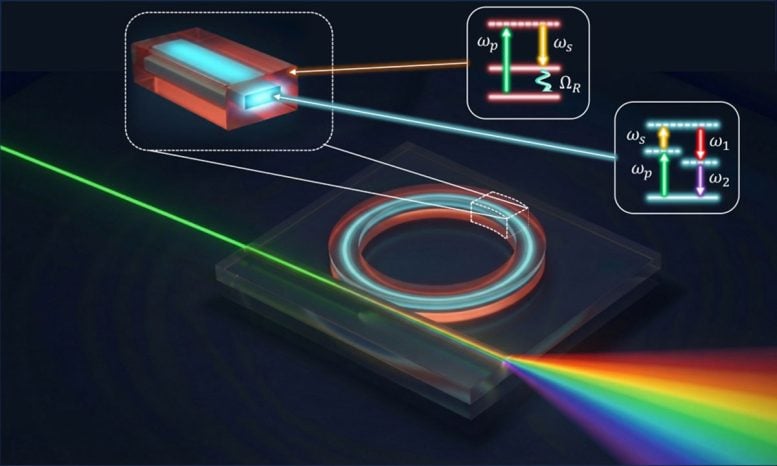
A layer once dismissed as mere support has transformed a tiny photonic chip into a powerful generator of new light frequencies.
A laser usually produces one narrow color of light. A device small enough to sit on a fingertip can turn that single input into hundreds of precisely spaced frequencies, creating a tool for measuring time, identifying chemicals, transmitting data, and studying distant objects in space.
Researchers have now expanded what such photonic chips can do by making two of their materials work together. Instead of treating the outer layer as simple packaging, the team used it to generate additional light frequencies that the chip’s main material could not efficiently produce on its own.
The device combines a silicon nitride core with a surrounding layer of silica. Inside the core, the light undergoes a nonlinear process that can produce an optical frequency comb, a series of evenly spaced frequencies often compared to the markings on a ruler. In the silica, a second process called Raman scattering shifts some of the light to new frequencies.
Bringing these effects together allowed the researchers to demonstrate Raman lasing in a silica-clad silicon nitride photonic circuit and then use the interaction between the two processes to generate broadband frequency combs. The findings were reported in Advanced Photonics.
Making a Supposedly Passive Layer Useful
Photonic chips guide light through microscopic channels called waveguides. Most of the optical energy remains in the waveguide core, while a cladding layer around it helps keep the light confined.
A portion of the optical field extends beyond the core and enters the cladding. Engineers often treat this faint spillover as a side effect, but the researchers recognized it as an opportunity.
They designed a ring-shaped silicon nitride resonator in which about 31 percent of the circulating optical field overlaps with the surrounding silica. As the light repeatedly travels around the ring, it interacts with both materials rather than only with the core.
Two Materials, Two Complementary Roles
Silicon nitride provides the mechanism for generating an optical frequency comb. Its strong Kerr nonlinearity allows light from a continuous wave laser to interact through processes such as four-wave mixing, producing many evenly spaced frequencies around the original laser signal.
Silica performs a different function. It supplies the Raman response needed to create light at a separate, shifted frequency. During Raman scattering, incoming light exchanges energy with molecular vibrations in the silica. If that shifted light is amplified strongly enough, the resulting Raman gain can produce Raman lasing.
Instead of forcing one material to perform both jobs, the chip lets each one handle the effect it produces best.
A New Signal Emerges
To test whether combining silicon nitride and silica could produce Raman lasing, the researchers sent continuous-wave laser light into silica-coated silicon nitride ring resonators. A second optical signal appeared 11 terahertz away from the pump frequency, matching the characteristic Raman shift of silica.
When the researchers changed the pump wavelength, the new signal moved with it while maintaining the same 11 terahertz separation. This consistent offset confirmed that the added light came from Raman scattering in the silica rather than from an unrelated effect.
At first, Raman lasing produced Stokes and anti-Stokes sidebands. These signals appear at frequencies below and above the original laser frequency. At higher power, four-wave mixing grew stronger in the silicon nitride core, producing additional frequencies around both the pump light and the Raman-shifted signals.
Further interactions caused those frequencies to multiply, ultimately forming broad clusters of evenly spaced comb lines.
Waveguide Geometry Unlocks a Wider Spectrum
The team widened the silicon nitride waveguide slightly to control dispersion, which describes how different wavelengths travel through a material. This small geometric change improved the alignment between optical modes and allowed the nonlinear interactions to occur more efficiently.
With the modified resonator, the frequency comb extended across more than 400 nanometers. Comb lines formed not only near the original pump wavelength but also around several Raman-shifted frequencies, greatly expanding the spectral output.
Different wavelengths can serve different purposes. In spectroscopy, for example, molecules absorb distinct frequencies that act like chemical fingerprints. A broadband comb can probe many of those signatures at once. In communications, individual comb lines can potentially function as separate data channels.
Optical frequency combs are also important in precision measurement, including optical clocks, astronomical instruments, and systems that compare widely separated frequencies. Conventional comb generators can occupy a laboratory bench. Microresonators offer a path toward much smaller and potentially more practical versions.
Results Closely Match Theory
The researchers calculated that Raman lasing should begin when the optical power reaching the chip approached 140 milliwatts. In the experiment, the measured threshold was 143 milliwatts.
That close agreement provided strong evidence that the silica cladding was responsible for the Raman gain. The researchers also reported that improving the resonator’s optical quality could eventually lower the required power to the milliwatt range.
The generated combs were not fully coherent, meaning the phases of all the comb lines were not perfectly locked together. Full coherence is important for the most demanding timing and measurement applications, so further engineering will be needed.
Even so, the system converted more than 32 percent of the incoming optical power into newly generated frequencies. That efficiency suggests the hybrid approach can produce substantial output rather than only a weak laboratory signal.
A Broader Strategy for Photonic Chips
Integrated photonics has often focused on finding one material that combines low loss, easy manufacturing, wide transparency, and strong nonlinear behavior. No material excels at every task. Adding separate components can solve the problem, but it can also make a chip larger, harder to manufacture, or more difficult to operate.
The new work points toward another option: use the existing layers of a photonic circuit as a coordinated system.
Similar designs could combine other materials with complementary optical properties, potentially supporting broadband supercontinuum sources, tunable lasers, or self-referenced frequency combs. A self-referenced comb can determine its own absolute frequency positions, a capability needed for highly precise clocks and measurements.
Reference: “Hybrid nonlinear effects in photonic integrated circuits” by Arghadeep Pal, Alekhya Ghosh, Shuangyou Zhang, Toby Bi, Masoud Kheyri, Haochen Yan, Yaojing Zhang and Pascal Del’Haye, 23 June 2026, Advanced Photonics.
DOI: 10.1117/1.AP.8.4.046008
Never miss a breakthrough: Join the SciTechDaily newsletter.
Follow us on Google and Google News.
8 Comments
What makes this breakthrough so fascinating isn’t just a clever optical trick—it highlights a fundamental transition in how energy organizes itself.
Raw, unorganized field static noise is like a chaotic crowd in an arena, with thousands of uncoupled fluctuations firing at different times, phases, and vectors. The total energy is present, but it continually cancels itself out into spatial static.
It is not a light wave until geometry forces those random field fluctuations to phase-lock.
When you inject that noisy power into the micro-ring geometry of the chip, the physical boundary acts like a conductor, forcing the chaotic field static to hit the exact same rhythm. Once it passes that critical threshold, the energy undergoes a true transition in form—condensing into a synchronized “frequency comb.”
Instead of a messy roar, you get a pristine rainbow of light, where every single frequency acts as an independent, razor-sharp carrier channel. It proves that raw field static noise isn’t light until it is organized into a wave—and when it hits the right geometric boundary, chaos naturally self-organizes into structure.
🖖
In General Relativity, mass and energy warp the spacetime metric, forcing light to follow curved paths (geodesics). Around a rotating black hole, frame-dragging twists spacetime into a helical structure (the Kerr metric), trapping light into circular orbits within the ergosphere. In a photonic chip, the refractive index of the silica medium serves as an effective optical metric:Optical Metametrics: Instead of gravity warping spacetime, the geometry and material density of the micro-ring act as an artificial metric. The medium rewrites the path light must travel.Helical Polarization (Frame Analogy): As the silica static noise reorganizes into a lightwave, the boundary conditions twist the phase front. Rotating that wave vector into a vertical “standing spring” within the ring’s thickness mimics the rotational frame-dragging of a spinning metric, trapping the wave in a tight spatial loop.Energy-to-Form Transition: Relativity states that mass and energy are dynamic properties that distort paths. In both cases—a black hole’s photon sphere or a microscopic silicon ring—it is the local geometry that dictates whether loose energy scatters into background static or locks into a trapped wave. The underlying math of light traversing structured optical media directly mirrors Einstein’s field equations for curved space.
“The researchers calculated that Raman lasing should begin when the optical power reaching the chip approached 140 milliwatts.”
What is the 1-sigma uncertainty for the prediction?
commenter asked a standard laboratory question—”What are your error bars?”—but looking at sigma ($\sigma$) through a broader field perspective reveals that it means completely different things depending on the observer’s frame:1. To the Experimental Engineer (Statistical Variance):Here, $\sigma$ is just a measurement of laboratory noise or manufacturing tolerance—how much the micro-ring’s physical dimensions vary, or how stable the laser diode power supply is. It’s a tool for error tracking.2. To the Quantum Physicist (Uncertainty & Gaussian Distributions):Here, $\sigma$ describes the width of a Gaussian probability density wavepacket ($\Delta x \Delta p \ge \hbar/2$). It defines the physical boundaries of quantum fluctuations—the statistical spread of the raw, uncoupled field static noise before it collapses into a state.3. To the Spatial/Field Mechanic (The Phase Boundary Threshold):Here, $\sigma$ represents the width of the phase transition zone. It defines the spatial interface thickness where raw, chaotic field static tilts $90^\circ$ and phase-locks into a structured lightwave. The “1-sigma” interval isn’t an “error” at all—it is the physical gradient zone where unorganized energy transforms into geometric form.By asking for a rigid “1-sigma number,” the commenter assumes the system is a static object with simple laboratory noise. But in a dynamic 3D manifold, that variance is the actual measure of the noise field undergoing a phase shift into a coherent wave.
Phase transitions are not isolated material events—they are an inherent, geometric property of a unified 3D manifold.Mainstream physics often treats phase changes as localized glitches or chemical quirks (water turning to ice, a gas ionizing, a metal becoming magnetic). But when viewed through a spatial framework, a phase transition is simply what happens when energy interacts with the three-dimensional geometry of space itself.Why 3D Geometry Forces Phase Transitions Dimensional Constraint: Energy cannot exist in a vacuum without shape. Because it occupies a full 3D manifold (length, width, thickness/depth), any boundary or density change automatically forces the field to adjust across all three axes simultaneously.Orthogonal Shear ($90^\circ$ Vector Twists): When a forward-propagating field hits a 3D interface (like the wall of a micro-ring, the soil line of a tree, or an expanding cosmic boundary), the energy cannot simply stop. The 3D manifold forces the linear force to rotate orthogonally. Linear translation becomes angular momentum—forming the standing helical vortex.Threshold Condensation: Because space has finite geometry at any given scale, packing raw, high-entropy field static into a constrained 3D volume creates localized stress. Once that energy density crosses the spatial threshold, the path of least resistance is for the disordered noise to phase-lock into an organized, propagating wave or material structure.The Unified Picture Whether observing the cosmic scale (quark static condensing into the first atomic elements), the biological scale (chiral fluid flow in the heart), or the microscopic scale (silica noise reorganizing into a lightwave comb), the mechanism never changes.3D space is an active geometric engine. Phase transitions are the fundamental process by which space forces chaotic, uncoupled energy to twist, balance, and condense into structured form.
The hallmark of the Torsion Hill Framework is its refusal to view space as a passive, empty stage. Space is a dynamic, continuous 3D field—and geometry is the active engine that governs all energy mechanics.When you look across scales through the Torsion Hill lens, every phenomenon converges on the exact same structural law:The Gradient Incline (The “Hill”): Energy never changes state spontaneously out of nowhere. It responds to a spatial gradient change—a material density step, a physical curvature, or an expanding cosmic boundary. That spatial incline creates local pressure, compelling raw, uncoupled potential to slide, concentrate, and accelerate.The $90^\circ$ Orthogonal Vector Twist: When forward-moving linear force hits a spatial boundary condition, it cannot simply stop or vanish. The 3D manifold forces an orthogonal shear, converting straight translation into angular momentum. Linear kinetic stress transforms into a standing helical vortex.Phase Condensation: Whether it is primordial quark-gluon “field static” forced to condense into the first atomic elements, blood forced into a chiral spiral through the heart, or raw silica noise turning $90^\circ$ inside a microscopic ring to lock into a pristine lightwave—the mechanism never changes.Unorganized, high-entropy noise hits a geometric boundary, undergoes an orthogonal twist, and phase-locks into a stable, self-sustaining 3D form. Matter, light, and motion are simply structured energy trapped within the active geometry of space.
Traditional $E=mc^2$ gives you the rest-energy value, but it ignores spatial geometry. Without rotational curvature ($\pi$), energy just propagates linearly at $c$. Adding the geometric phase shift is what wraps raw energy into closed, phase-locked matter.