Solar start-up company Ampuse has teamed up with NREL and ORNL to reduce the cost of solar cells through the use of a new manufacturing process, a chemical vapor deposition process to grow the silicon on inexpensive foil. By doing away with silicon wafers, the Ampuse model will have the potential to produce a 15%-efficient solar cell at less than 50 cents per watt.
Solar-powered electricity prices could soon approach those of power from coal or natural gas thanks to collaborative research with solar start-up Ampulse Corporation at the U.S. Department of Energy’s (DOE) National Renewable Energy Laboratory (NREL).
Silicon wafers account for almost half the cost of today’s solar photovoltaic (PV) panels, so reducing or eliminating wafer costs is essential to bringing prices down.
Current crystalline silicon technology, while high in energy conversion efficiency, involves processes that are complex, wasteful, and energy intensive. First, half the refined silicon is lost as dust in the wafer-sawing process, driving module costs higher. A typical 2-meter boule of silicon loses as many as 6,000 potential wafers during sawing. Second, the wafers produced are much thicker than necessary. To efficiently convert sunlight into electricity, they need only one-tenth the typical thickness.

NREL, DOE’s Oak Ridge National Laboratory (ORNL), and Ampulse have teamed on an approach to eliminate this waste and dramatically lower the cost of the finished solar panels. The aim is to create a less expensive alternative to wafer-based crystalline silicon solar cells.
By using a chemical vapor deposition process to grow the silicon on inexpensive foil, Ampulse is able to make the solar cells just thick enough to convert most of the solar energy into electricity. No more sawdust — and no more wasting refined silicon materials.
Straight from Pure Silicon to High-Quality Crystal Silicon Film
NREL developed the technology to grow high-quality silicon.
ORNL developed the metal foil that has the correct crystal structure to support that growth.
And Ampulse is installing a pilot manufacturing line in NREL’s Process Development Integration Laboratory (PDIL), where solar companies test their latest materials and processes.
With knowledge and expertise acquired from the PDIL pilot production line, Ampulse plans to design a full-scale production line to accommodate long rolls of metal foil.
The Ampulse process “goes straight from pure silicon-containing gas to high-quality crystal silicon film,” said Brent Nelson, who runs the PDIL at NREL. “The advantage is you can make the wafer just as thin as you need it — 10 microns or less.”
Most of today’s solar cells are made out of wafer crystalline silicon, though thin-film cells made of more exotic materials like gallium, arsenic, indium, arsenide, cadmium, and tellurium are making a strong push into the market.
The advantage of silicon is its abundance, as it is derived from sand. Its disadvantage is that purifying it into wafers suitable for solar cells is expensive and energy intensive.

Manufacturers add carbon and heat to sand to produce metallurgical-grade silicon, which is useful in other industries, but not yet suitable for making solar cells. This metallurgical-grade silicon is then converted to pure trichlorosilane (SiCl3) or silane (SiH4) gas.
Typically, the purified gas is converted to create a silicon feedstock at 1,000 degrees Celsius (°C). This feedstock is melted at 1,414°C and recrystallized into crystal ingots that are finally sawed into wafers. Think of it as the Rube Goldberg approach to creating a solar cell.
Instead, the Ampulse process backs up two steps. Rather than create a feedstock, it works with the silane directly and grows just the needed silicon right onto a foil substrate.
Combining NREL’s Deposition Technique with ORNL’s Textured Foil
A team of NREL scientists including Howard Branz and Chaz Teplin had developed a way to use a process called hot-wire chemical vapor depositionPDF to thicken silicon wafers with perfect crystal coatings. Using a hot tungsten filament much like the one found in an incandescent light bulb, the silane gas molecules are broken apart and deposited onto the wafer using the chemical vapor deposition technique at about 700°C — a much lower temperature than needed to make the wafer. The hot filament decomposes the gas, allowing silicon layers to deposit directly onto the substrate.
Armed with this new technique, Branz and Teplin searched for ways to grow the silicon on cheaper materials and still use it for solar cells.

They found the ideal synergy when visiting venture capitalists from Battelle Ventures asked them whether they could do anything useful with a breakthrough at ORNL called RABiTS (rolling assisted biaxially textured substrate). It was just the opportunity the two scientists had been seeking.
If metal foil is to work as a substrate, it must be able to act as a seed crystal so the silicon can grow on it with the correct structure. The RABiTS process forms crystals in the foil that are correctly oriented to receive the silicon atoms and lock them into just the right positions.
NREL and ORNL worked to combine their technologies using a small amount of funding from Battelle Ventures. Using the right intermediate “buffer layers” to coat the foil substrates, the researchers were able to replicate the desired foil crystal structure in the silicon layer grown over metal foil (epitaxial growth).
Establishing Ampulse Corporation
With a commitment to develop the new technology in cooperation with the two national labs, Battelle Ventures and Innovation Valley Partners joined forces to form Ampulse. Initially, Ampulse had very few employees and no offices — just a name, an idea, and a commitment to develop the technology via the unique instrumentation and scientific expertise at the two national labs.
The company then established a $500,000 cooperative research and development agreement (CRADA) with NREL and a similar agreement with ORNL.
Ampulse also received a total of $900,000 from DOE’s Technology Commercialization and Deployment funds at NREL and ORNL. Because Ampulse was started as a company with very low overhead, nearly all its initial funding went toward research efforts at NREL and ORNL.
“Our initial technology success from those funds enabled Ampulse to raise two rounds of venture capital,” Branz said.
The company now has 13 employees and six full-time consultants and is currently working with 22 sponsored researchers from two national labs. The first employee at Ampulse, Steve Hane, remains its CEO.
A Giant Step Toward the $1 per Watt Goal?
“We have the potential to produce a 15%-efficient solar cell at less than 50 cents per watt with a fraction of the capital investment of other venture-funded PV companies,” Hane said. “And that’s due to our R&D collaborations with the national labs.” Hane said the unique relationship between the national labs and venture capitalists should be a model for future technology transfers to the private sector.
Recently, with its SunShot Initiative, DOE challenged researchers to lower the cost of solar energy by two-thirds to $1 per watt installed. By eliminating costly silicon wafers — but still using silicon as the core material — the Ampulse approach has the potential to meet this target.
“The trick is to get as good material quality as you have in a wafer,” Teplin said. “We’re using our existing knowledge of how to grow silicon directly from a gas phase onto these metal foils.”
Production Line Features Vacuum Chambers and Quartz Lamps
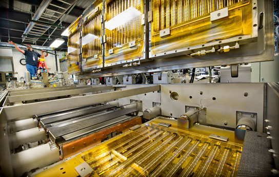
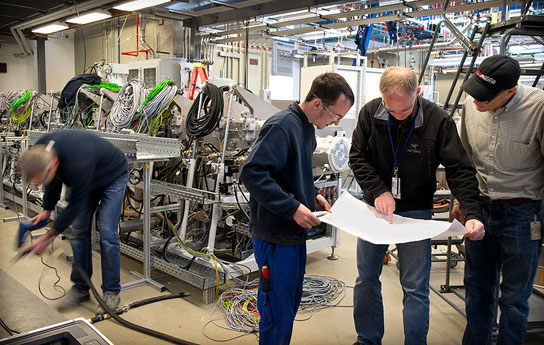
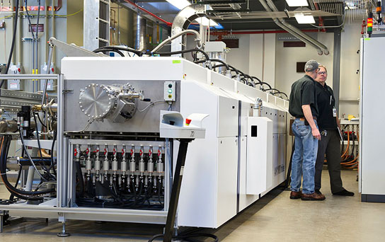
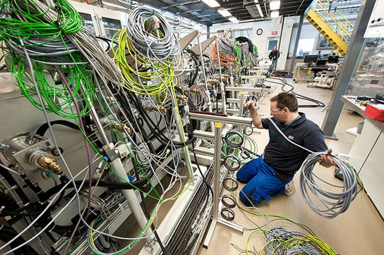
The production line being installed at NREL’s PDIL consists of a half dozen cube-like vacuum chambers where foils are overcoated with buffer and silicon layers to fabricate solar cells. It was built to Ampulse’s specifications by Roth & Rau Microsystems of Germany.
The new production system will also exchange samples with other NREL research and analysis equipment in the PDIL. NREL’s “wafer replacement tool” will be connected to the Ampulse system and will have a robot that can retrieve samples while maintaining vacuum, preventing exposure of the sample to air.
To fabricate solar cells, metal foils are loaded into the Ampulse system, where quartz lamps heat them to a temperature of 850°C. First, the foils are coated with the necessary buffer layers. Then, the samples are transferred to a specially designed chamber where the key silicon layers are grown. The silicon is then exposed to atomic hydrogen to improve its electronic properties. Finally, solar cell junction and electrical contacts are developed.
“With this new tool, we will be able integrate NREL and ORNL technologies seamlessly and quickly,” Teplin said. “Further, with access to all of NREL’s other PDIL capabilities, we really expect technological progress to accelerate.”
Branz summed up: “The main thing is that we can grow high-quality silicon layers very fast and without putting much energy into the process. That means the solar cells can turn out much cheaper than the wafer-based cells.”
“Our process goes directly from gas to the epitaxial silicon phase, bypassing the growth and sawing phase,” Ampulse’s Director of Planning and Logistics, Mike Colby, said. “We made it large because we needed to demonstrate the scalability of the system.”
“To accelerate time to market, we need to maximize the cycle speed,” Colby added. “The goal is to achieve the crystal silicon performance that until now focused on thicker wafers — and without having to use a 1,400°C furnace.”
As skilled technicians tweaked the knobs of the potentially game-changing prototyping line, Colby said, “We’ve had good luck and a good relationship with NREL. The aim of NREL, and of the PDIL, is to work with the needs of business and help accelerate commercialization of new technologies. This definitely does that.”
Never miss a breakthrough: Join the SciTechDaily newsletter.
Follow us on Google and Google News.