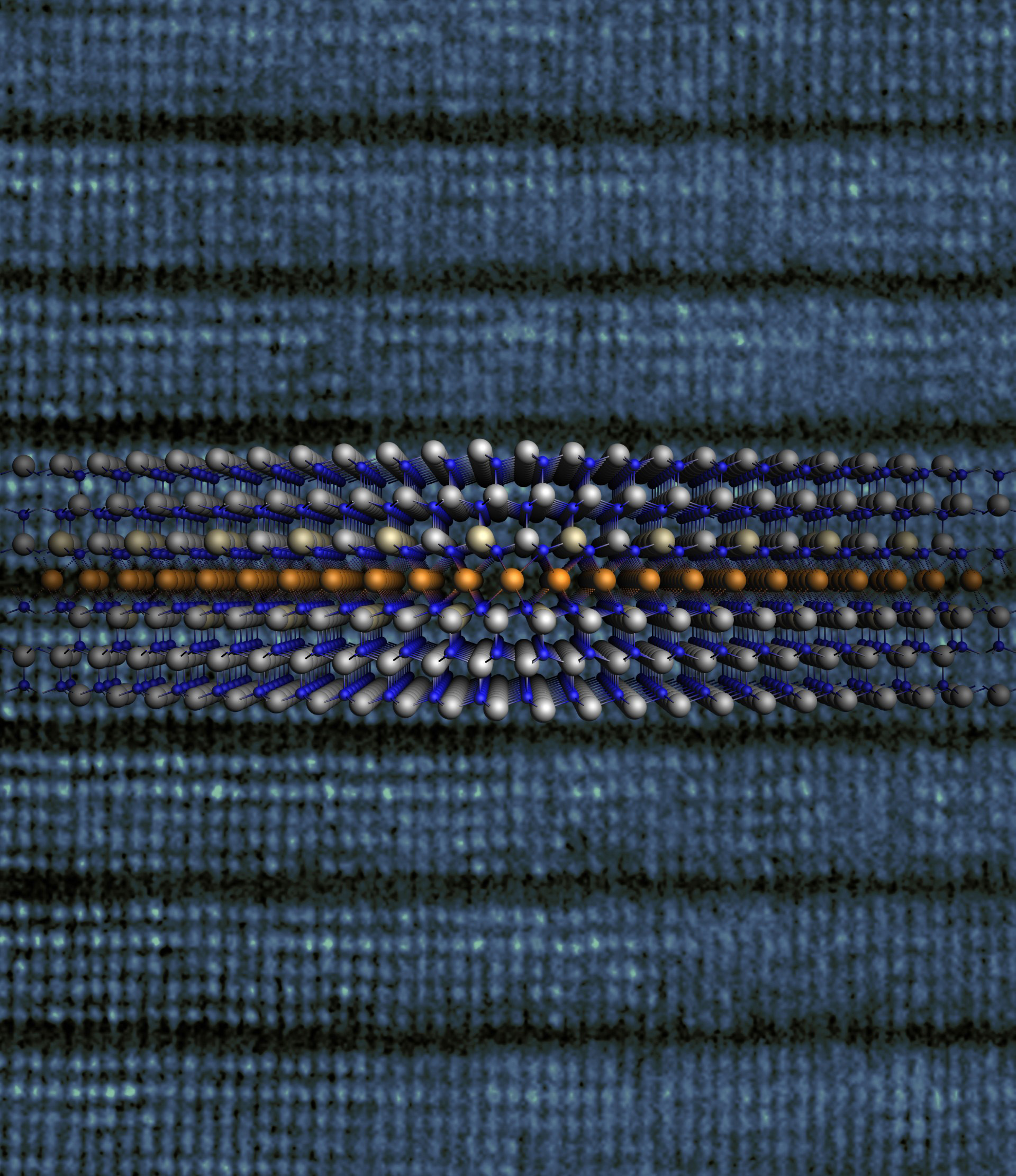
Thermal treating of metallic magnesium on gallium nitride semiconductors results in the formation of a distinctive superlattice structure. Magnesium, nitrogen, and gallium atoms are shown in orange, blue, and grey, respectively. Credit: Jia Wang
New research has discovered a new superlattice structure in gallium nitride (GaN) using magnesium (Mg), promising advancements in semiconductor performance.
A new study has revealed a new superlattice structure in gallium nitride (GaN) by combining it with magnesium (Mg), potentially enhancing GaN-based semiconductor devices and advancing the field of elastic strain engineering.
A study led by Nagoya University in Japan revealed that a simple thermal reaction of gallium nitride (GaN) with metallic magnesium (Mg) results in the formation of a distinctive superlattice structure. This represents the first time researchers have identified the insertion of 2D metal layers into a bulk semiconductor.
By carefully observing the materials through various cutting-edge characterization techniques, the researchers uncovered new insights into the process of semiconductor doping and elastic strain engineering. They published their findings in the journal Nature.
GaN is an important wide bandgap semiconductor material that is poised to replace traditional silicon semiconductors in applications demanding higher power density and faster operating frequencies. These distinctive characteristics of GaN make it valuable in devices such as LEDs, laser diodes, and power electronics—including critical components in electric vehicles and fast chargers. The improved performance of GaN-based devices contributes to the realization of an energy-saving society and a carbon-neutral future.
Understanding Electrical Conductivity in Semiconductors
In semiconductors, there are two essential and complementary types of electrical conductivity: p-type and n-type. The p-type semiconductor features primarily free carriers carrying positive charges, known as holes, whereas the n-type semiconductor conducts electricity through free electrons.
A semiconductor acquires p-type or n-type conductivity through a process called doping, which refers to the intentional introduction of specific impurities (known as dopants) into a pure semiconductor material to greatly alter its electrical and optical properties.
In the field of GaN semiconductors, Mg is the only known element to create p-type conductivity up to now. Despite 35 years since the first success of doping Mg into GaN, the full mechanisms of Mg doping in GaN, especially the solubility limit and segregation behavior of Mg, remain unclear. This uncertainty limits their optimization for optoelectronics and electronics.
Experimentation and Observations
To improve the conductivity of p-type GaN, Jia Wang, the first author of the study, and his colleagues conducted an experiment in which they patterned deposited metallic Mg thin films on GaN wafers and heated them up at a high temperature—a conventional process known as annealing.
Using state-of-the-art electron microscope imaging, the scientists observed the spontaneous formation of a superlattice featuring alternating layers of GaN and Mg. This is especially unusual since GaN and Mg are two types of materials with significant differences in their physical properties.
“Although GaN is a wide-bandgap semiconductor with mixed ionic and covalent bonding, and Mg is a metal featuring metallic bonding, these two dissimilar materials have the same crystal structure, and it is a strikingly natural coincidence that the lattice difference between hexagonal GaN and hexagonal Mg is negligibly small,” Wang said. “We think that the perfect lattice match between GaN and Mg greatly reduces the energy needed to create the structure, playing a critical role in the spontaneous formation of such a superlattice.”
The scientists determined that this unique intercalation behavior, which they named interstitial intercalation, leads to compressive strain to the host material. Specifically, they found that the GaN being inserted with Mg layers sustains a high stress of more than 20 GPa, equivalent to 200,000 times atmospheric pressure, making it the highest compressive strain ever recorded in a thin-film material. This is much more than the compressive stresses commonly found in silicon films (in the range of 0.1 to 2 GPa). Electronic thin films can undergo significant changes in electronic and magnetic properties because of this strain. The researchers found that the electrical conductivity in GaN via hole transport was significantly enhanced along the strained direction.
“Using such a simple and low-cost approach, we were able to enhance the transport of holes in GaN, which conducts more current,” Wang said. “This interesting finding in interactions between a semiconductor and a metal may provide new insights into semiconductor doping and improve the performance of GaN-based devices.”
Nagoya University and GaN
The fact that this study took place at Nagoya University is fitting, considering its reputation as the “cradle of GaN technology.” Hiroshi Amano, the corresponding author of the current study, and Isamu Akasaki from Nagoya University developed the first blue-light LEDs in the late 1980s, employing Mg-doped GaN. Their contributions, for which they received the Nobel Prize in Physics in 2014, have played an important role in creating a more energy-efficient society.
“The discovery of Mg-intercalated GaN superlattice structures and the identification of the novel mechanism of 2D-Mg doping offer a hard-earned opportunity to honor the pioneering achievements in the field of III-nitride semiconductor research,” said Wang. Having advanced the technology 10 years after the Nobel Prize, Wang referred to this timely finding as a “true gift of nature” that could potentially open new avenues and inspire more basic research in this field.
Reference: “Observation of 2D-magnesium-intercalated gallium nitride superlattices” by Jia Wang, Wentao Cai, Weifang Lu, Shun Lu, Emi Kano, Verdad C. Agulto, Biplab Sarkar, Hirotaka Watanabe, Nobuyuki Ikarashi, Toshiyuki Iwamoto, Makoto Nakajima, Yoshio Honda and Hiroshi Amano, 5 June 2024, Nature.
DOI: 10.1038/s41586-024-07513-x
The Japan Science and Technology Agency supported the research through the ASPIRE program and AdCORP Program grants. This project also received support from the Ministry of Education, Culture, Sports, Science, and Technology of Japan, the Ministry of Economics, Trade and Industry, and Japan Society for the Promotion of Science.


Be the first to comment on "“True Gift of Nature” – Discovery of Unique New Superlattice Unveils New Semiconductor Doping Mechanism"