Researchers in Japan have integrated niobium nitride with aluminum nitride substrates, enabling superconducting qubits to be manufactured using existing silicon processes.
Computers that can use quantum mechanics’ “spooky” properties to solve problems quicker than existing technology may seem appealing, but they must first overcome a major obstacle. Scientists from Japan may have discovered the solution by demonstrating how a superconducting material, niobium nitride, can be added as a flat, crystalline layer to a nitride-semiconductor substrate. This technique could make it simple to manufacture quantum qubits that can be used with conventional computer devices.
Conventional silicon microprocessor manufacturing techniques have grown over decades and are continually being refined and enhanced. On the other hand, the majority of quantum computing architectures must be created mostly from scratch. However, discovering a technique to integrate quantum and conventional logic units on a single chip, or even adding quantum capabilities to existing fabrication lines, might greatly hasten the adoption of these new systems.
Innovative Use of Niobium Nitride in Quantum Devices
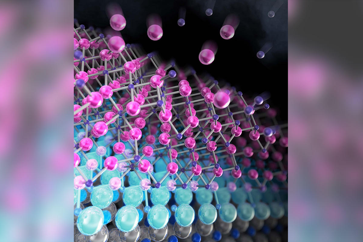
Recently, a group of scientists from The University of Tokyo’s Institute of Industrial Science demonstrated how thin films of niobium nitride (NbNx) can grow directly on top of an aluminum nitride (AlN) layer. Niobium nitride can become superconducting at temperatures colder than 16 degrees Celsius above absolute zero. Because of this, it can be utilized to create a superconducting qubit when arranged in a structure called a Josephson junction.
The scientists investigated the impact of temperature on the crystal structures and electrical properties of NbNx thin films grown on AlN template substrates. They showed that the spacing of atoms in the two materials was compatible enough to produce flat layers.
“We found that because of the small lattice mismatch between aluminum nitride and niobium nitride, a highly crystalline layer could grow at the interface,” says first and corresponding author Atsushi Kobayashi.
The crystallinity of the NbNx was characterized with X-ray diffraction, and the surface topology was captured using atomic force microscopy. In addition, the chemical composition was checked using X-ray photoelectron spectroscopy. The team showed how the arrangement of atoms, nitrogen content, and electrical conductivity all depended on the growth conditions, especially the temperature.
“The structural similarity between the two materials facilitates the integration of superconductors into semiconductor optoelectronic devices,” says Atsushi Kobayashi.
Moreover, the sharply defined interface between the AlN substrate, which has a wide bandgap, and NbNx, which is a superconductor, is essential for future quantum devices, such as Josephson junctions. Superconducting layers that are only a few nanometers thick and have high crystallinity can be used as detectors of single photons or electrons.
Reference: “Crystal-Phase Controlled Epitaxial Growth of NbNx Superconductors on Wide-Bandgap AlN Semiconductors” by Atsushi Kobayashi, Shunya Kihira, Takahito Takeda, Masaki Kobayashi, Takayuki Harada, Kohei Ueno and Hiroshi Fujioka, 21 September 2022, Advanced Materials Interfaces.
DOI: 10.1002/admi.202201244
Never miss a breakthrough: Join the SciTechDaily newsletter.
Follow us on Google and Google News.