
Researchers are advancing energy-efficient supercomputing by harnessing charge density waves in materials, a technique that mimics brain neurons. New microscopy methods at Argonne National Laboratory are revealing how these waves can be manipulated through electricity, offering insights into faster, smaller, and more efficient microelectronic devices. Credit: SciTechDaily.com
Charge density waves have applications in next-generation and energy-efficient computing.
Scientists used an ultrafast electron microscope to capture the nanosecond changes in a material during electrical pulsing. Understanding these changes may lead to more energy-efficient electronics.
Today’s supercomputers consume vast amounts of energy, equivalent to the power usage of thousands of homes. In response, researchers are developing a more energy-efficient form of next-generation supercomputing that leverages artificial neural networks. These networks mimic the processes of neurons, the basic unit in the human brain. This mimicry could be achieved through the charge density waves that occur in certain materials. Charge density waves are wave-like patterns of electrons — negatively charged particles — that move in a correlated fashion.
Unraveling the Dynamics of Charge Density Waves
The charge density waves increase the resistance to the movement of electrons in the material. The ability to control the waves could provide fast switching of the resistance on and off. This property could then be exploited for more energy-efficient computing, as well as ultraprecise sensing. However, it is not clear how the switching process occurs, especially given that the waves change from one state to another within 20 billionths of a second.
“This new technique produced results with broad applications to energy-efficient microelectronics.”
— Charudatta Phatak, materials scientist and deputy division director
Advancements in Microscopy at Argonne National Laboratory
Researchers at the U.S. Department of Energy’s (DOE) Argonne National Laboratory have found a new way to study these waves. To do so, they turned to the ultrafast electron microscope at the Center for Nanoscale Materials, a DOE Office of Science user facility at Argonne. They developed a new microscopy technique that uses electrical pulses to observe the nanosecond dynamics within a material that is known to form charge density waves at room temperature. That material is a tantalum sulfide referred to as 1T-TaS2.
The team tested a flake of this sulfide with two electrodes attached to generate electric pulses. During short pulses it was thought that the resulting high electric field or currents might drive the resistance switching. But two observations from the ultrafast electron microscope changed this understanding.
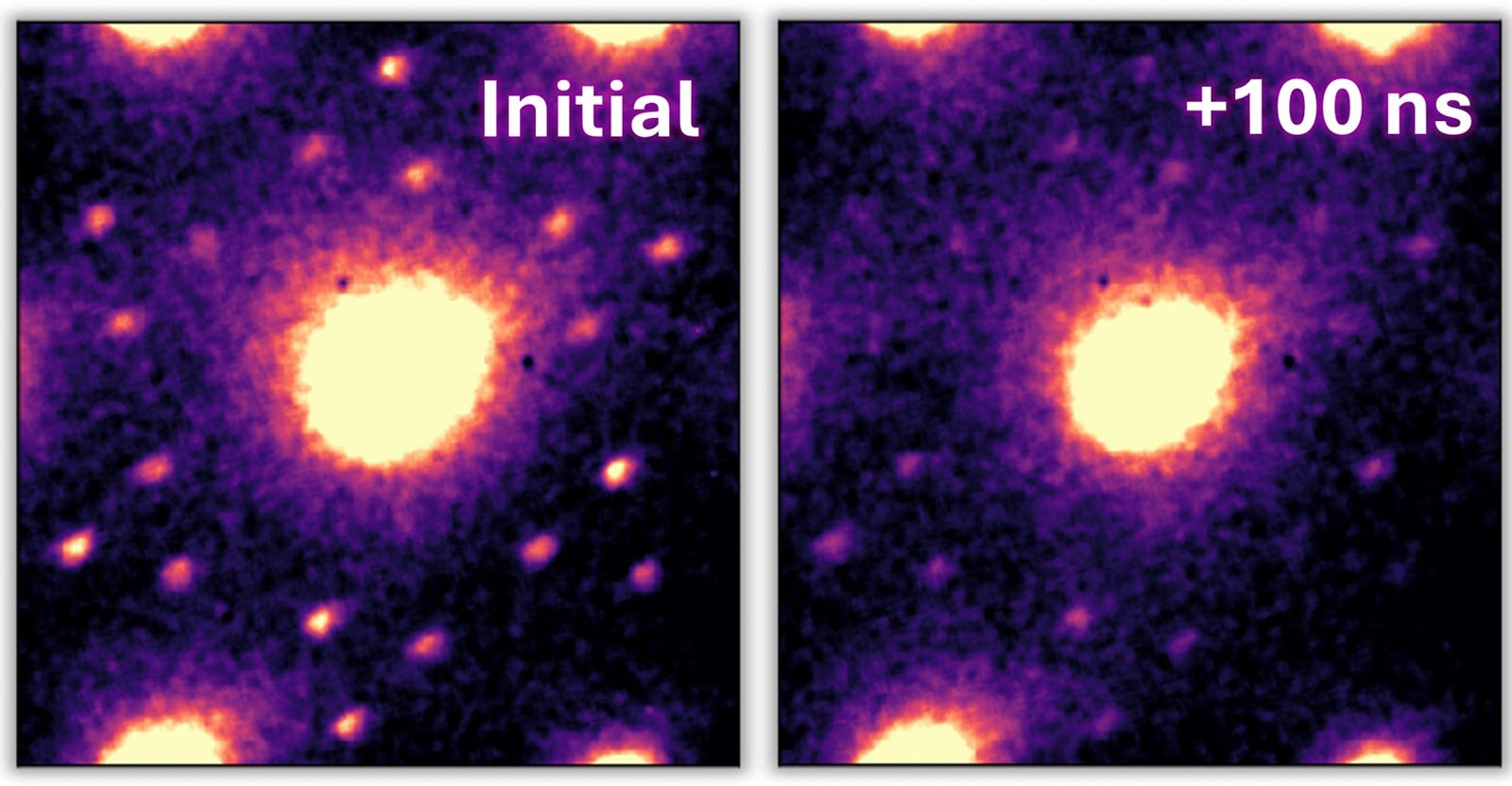
Diffraction patterns captured before and after a 20-nanosecond electrical pulse. The star-shaped pattern of small white spots, left, corresponds to the initial charge density wave pattern, which is temporarily melted by the heat from electrical pulse, right. Credit: Argonne National Laboratory
First, the charge density waves melted in response to the heat generated by the injected current rather than the charge current itself, even during nanosecond pulses. Second, the electrical pulses induced drum-like vibrations across the material, which wobbled the waves’ arrangement.
“Thanks to this new technique we determined these two previously unobserved ways in which electricity can manipulate the state of the charge density waves,” said Daniel Durham, a postdoctoral researcher at Argonne. “And the melting response mimics how neurons are activated in the brain, while the vibrational response could generate neuron-like firing signals in a neural network.”
This study demonstrates a new approach to examining these types of electrical switching processes. This ultrafast electron microscopy method allows researchers to observe how microelectronic materials function at nanoscale lengths and nanosecond speeds.
The drive toward smaller, faster, and more efficient microelectronic devices makes a material like 1T-TaS2 attractive. And its ability to be formed as a nanoscale layer also makes it appealing for such devices.
This new technique produced results with broad applications to energy-efficient microelectronics, according to Charudatta Phatak, a materials scientist and deputy division director at Argonne.
“Understanding the fundamental mechanisms of how we can control these charge density waves is important because this can be applied to other materials to control their properties,” Phatak said.
This research was published in Physical Review Letters.
Reference: “Nanosecond Structural Dynamics during Electrical Melting of Charge Density Waves in 1T−TaS2” by Daniel B. Durham, Thomas E. Gage, Connor P. Horn, Xuedan Ma, Haihua Liu, Ilke Arslan, Supratik Guha and Charudatta Phatak, 28 May 2024, Physical Review Letters.
DOI: 10.1103/PhysRevLett.132.226201
Besides Durham and Phatak, authors include Thomas Gage, Connor Horn, Xuedan Ma, Haihua Liu, Ilke Arslan and Supratik Guha. Horn and Guha have joint appointments at the University of Chicago.
This work was supported by the DOE Office of Science call for microelectronics research.


Be the first to comment on "Brain-Like Supercomputers: Harnessing Charge Density Waves for Revolutionary Efficiency"