Graphene Invisible to Water
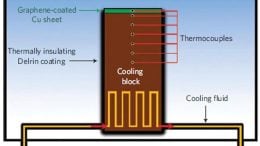
…not disrupted by graphene. This effect is an artifact of the extreme thinness of graphene—which is only about 0.3 nanometers thick,” Koratkar said. “Nothing can rival the thinness of graphene….
…not disrupted by graphene. This effect is an artifact of the extreme thinness of graphene—which is only about 0.3 nanometers thick,” Koratkar said. “Nothing can rival the thinness of graphene….

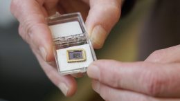
Graphene Flagship researchers have developed a new measurement standard for the analysis of graphene and layered materials that could accelerate production and optimize device fabrication. Credit: Graphene Flagship Graphene Flagship…

…large-area graphene films grown using chemical vapor deposition (CVD), correcting the mistaken consensus that grain boundaries of graphene are weak. In a new study, published in the journal Science on…
…an adhesive-like layer of nickel to peel graphene from silicon carbide, engineers at MIT have developed a technique to produce highly conductive wrinkle-free graphene wafers. Graphene has been touted as…

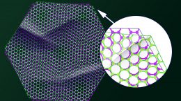
The Graphene Flagship analyses the current graphene landscape and market forecast for graphene over the following decade. Graphene is light, flexible, conductive, and one of the strongest materials in the…
…graphene” technique can convert a ton of coal, waste food or plastic into graphene for a fraction of the cost used by other bulk graphene-producing methods. “This is a big…
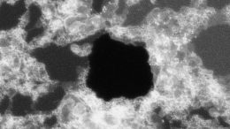
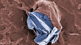
The researchers’ membrane, consisting of graphene on a polycarbonate track etch membrane (the graphene is the darker region in the center of the white film). The total membrane is about…
…named laser-induced graphene. Most carbon-containing materials can be converted into graphene using a commercial CO2 infrared laser system. Credit: City University of Hong Kong Graphene is known for its anti-bacterial…
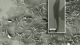
…strips of high-quality graphene. The team’s results are the first demonstration of an industrial, scalable method for manufacturing high-quality graphene that is tailored for use in membranes that filter a…
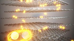
…graphene as a new “family” of robust superconductors, each member consisting of alternating graphene layers, stacked at precise angles. Credit: Courtesy of the researchers “The magic-angle graphene system is now…
…meantime, researchers have discovered more 2D materials, such as graphene-derived graphene acid, graphene oxide, and cyanographs, which could have applications in medicine. Researchers want to use inorganic 2D materials such…
In this illustration, two sheets of graphene are stacked together at a slightly offset “magic” angle, which can become either an insulator or superconductor. “We placed one sheet of graphene…
…practical uses. Seeking an alternative, a team from MIT and Harvard University is looking to graphene oxide — graphene’s much cheaper, imperfect form. Graphene oxide is graphene that is also…
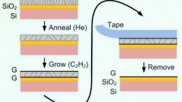
…carbon is deposited on the surface, where it forms layers of graphene above and beneath the SiO2. The top layer of graphene, attached to the nickel, easily peels away using…
…ballistic transport. Research reported this week shows that electrical resistance in nanoribbons of epitaxial graphene changes in discrete steps following quantum mechanical principles. The research shows that the graphene nanoribbons…
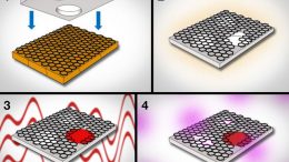
…seal large tears and defects in graphene. 4) Next, they use oxygen plasma to etch pores of specific sizes in graphene. Using graphene, researchers from MIT have developed a dialysis…
…other superconducting metals — an arrangement that allows graphene to inherit some superconducting behaviors. This time around, the team found a way to make graphene superconduct on its own, demonstrating…
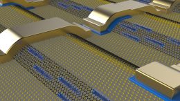
…functional semiconductor made from graphene. Graphene, characterized by a single layer of carbon atoms linked by the strongest bonds available, serves as the basis for this advancement. Semiconductors, essential materials…