For the first time, physicists have developed a technique that can peer deep beneath the surface of a material to identify the energies and momenta of electrons there.
The energy and momentum of these electrons, known as a material’s “band structure,” are key properties that describe how electrons move through a material. Ultimately, the band structure determines a material’s electrical and optical properties.
The team, at MIT and Princeton University, has used the technique to probe a semiconducting sheet of gallium arsenide, and has mapped out the energy and momentum of electrons throughout the material. The results are published today in the journal Science.
By visualizing the band structure, not just at the surface but throughout a material, scientists may be able to identify better, faster semiconductor materials. They may also be able to observe the strange electron interactions that can give rise to superconductivity within certain exotic materials.
“Electrons are constantly zipping around in a material, and they have a certain momentum and energy,” says Raymond Ashoori, professor of physics at MIT and a co-author on the paper. “These are fundamental properties which can tell us what kind of electrical devices we can make. A lot of the important electronics in the world exist under the surface, in these systems that we haven’t been able to probe deeply until now. So we’re very excited — the possibilities here are pretty vast.”
Ashoori’s co-authors are postdoc Joonho Jang and graduate student Heun Mo Yoo, along with Loren Pfeffer, Ken West, and Kirk Baldwin, of Princeton University.
Pictures beneath the surface
To date, scientists have only been able to measure the energy and momentum of electrons at a material’s surface. To do so, they have used angle-resolved photoemission spectroscopy, or ARPES, a standard technique that employs light to excite electrons and make them jump out from a material’s surface. The ejected electrons are captured, and their energy and momentum are measured in a detector. Scientists can then use these measurements to calculate the energy and momentum of electrons within the rest of the material.
“[ARPES] is wonderful and has worked great for surfaces,” Ashoori says. “The problem is, there is no direct way of seeing these band structures within materials.”
In addition, ARPES cannot be used to visualize electron behavior in insulators — materials within which electric current does not flow freely. ARPES also does not work in a magnetic field, which can greatly alter electronic properties inside a material.
The technique developed by Ashoori’s team takes up where ARPES leaves off and enables scientists to observe electron energies and momenta beneath the surfaces of materials, including in insulators and under a magnetic field.
“These electronic systems by their nature exist underneath the surface, and we really want to understand them,” Ashoori says. “Now we are able to get these pictures which have never been created before.”

Tunneling through
The team’s technique is called momentum and energy resolved tunneling spectroscopy, or MERTS, and is based on quantum mechanical tunneling, a process by which electrons can traverse energetic barriers by simply appearing on the other side — a phenomenon that never occurs in the macroscopic, classical world which we inhabit. However, at the quantum scale of individual atoms and electrons, bizarre effects such as tunneling can occasionally take place.
“It would be like you’re on a bike in a valley, and if you can’t pedal, you’d just roll back and forth. You would never get over the hill to the next valley,” Ashoori says. “But with quantum mechanics, maybe once out of every few thousand or million times, you would just appear on the other side. That doesn’t happen classically.”
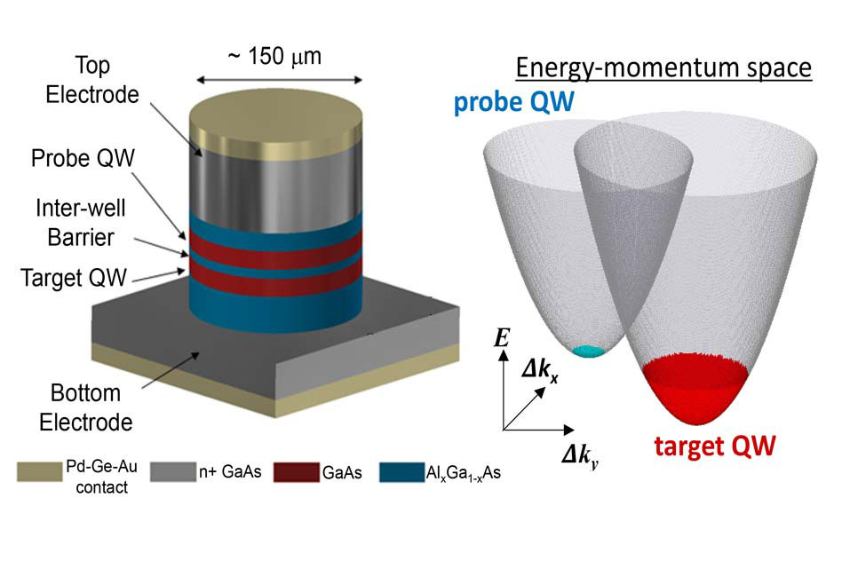
Ashoori and his colleagues employed tunneling to probe a two-dimensional sheet of gallium arsenide. Instead of shining light to release electrons out of a material, as scientists do with ARPES, the team decided to use tunneling to send electrons in.
The team set up a two-dimensional electron system known as a quantum well. The system consists of two layers of gallium arsenide, separated by a thin barrier made from another material, aluminum gallium arsenide. Ordinarily in such a system, electrons in gallium arsenide are repelled by aluminum gallium arsenide, and would not go through the barrier layer.
“However, in quantum mechanics, every once in a while, an electron just pops through,” Jang says.
The researchers applied electrical pulses to eject electrons from the first layer of gallium arsenide and into the second layer. Each time a packet of electrons tunneled through the barrier, the team was able to measure a current using remote electrodes. They also tuned the electrons’ momentum and energy by applying a magnetic field perpendicular to the tunneling direction. They reasoned that those electrons that were able to tunnel through to the second layer of gallium arsenide did so because their momenta and energies coincided with those of electronic states in that layer. In other words, the momentum and energy of the electrons tunneling into gallium arsenide were the same as those of the electrons residing within the material.
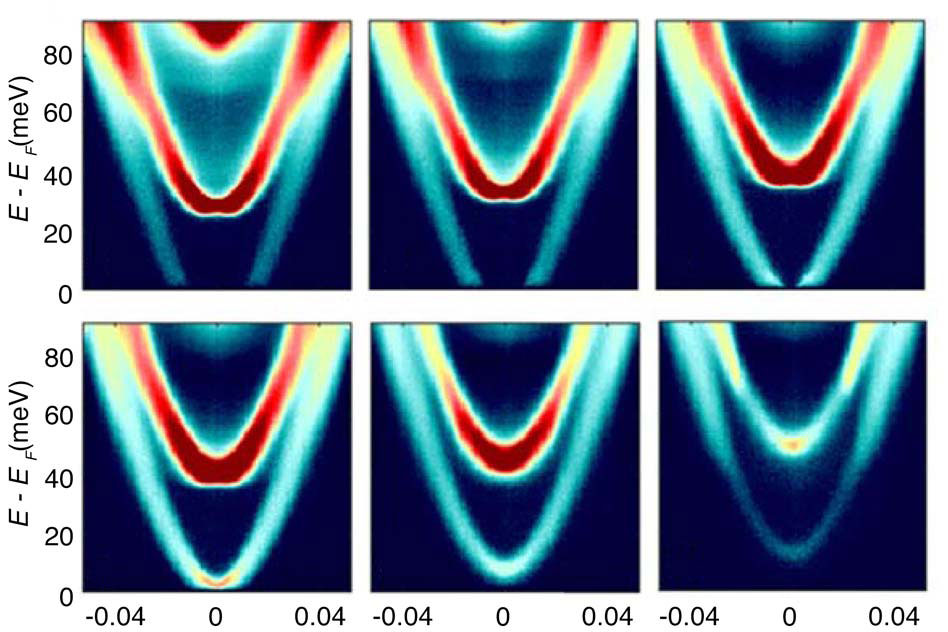
By tuning electron pulses and recording those electrons that went through to the other side, the researchers were able to map the energy and momentum of electrons within the material. Despite existing in a solid and being surrounded by atoms, these electrons can sometimes behave just like free electrons, albeit with an “effective mass” that may be different than the free electron mass. This is the case for electrons in gallium arsenide, and the resulting distribution has the shape of a parabola. Measurement of this parabola gives a direct measure of the electron’s effective mass in the material.
Exotic, unseen phenomena
The researchers used their technique to visualize electron behavior in gallium arsenide under various conditions. In several experimental runs, they observed “kinks” in the resulting parabola, which they interpreted as vibrations within the material.
“Gallium and arsenic atoms like to vibrate at certain frequencies or energies in this material,” Ashoori says. “When we have electrons at around those energies, they can excite those vibrations. And we could see that for the first time, in the little kinks that appeared in the spectrum.”
They also ran the experiments under a second, perpendicular magnetic field and were able to observe changes in electron behavior at given field strengths.
“In a perpendicular field, the parabolas or energies become discrete jumps, as a magnetic field makes electrons go around in circles inside this sheet,” Ashoori says.
“This has never been seen before.”
The researchers also found that, under certain magnetic field strengths, the ordinary parabola resembled two stacked donuts.
“It was really a shock to us,” Ashoori says.
They realized that the abnormal distribution was a result of electrons interacting with vibrating ions within the material.
“In certain conditions, we found we can make electrons and ions interact so strongly, with the same energy, that they look like some sort of composite particles: a particle plus a vibration together,” Jang says.
Further elaborating, Ashoori explains that “it’s like a plane, traveling along at a certain speed, then hitting the sonic barrier. Now there’s this composite thing of the plane and the sonic boom. And we can see this sort of sonic boom — we’re hitting this vibrational frequency, and there’s some jolt happening there.”
The team hopes to use its technique to explore even more exotic, unseen phenomena below the material surface.
“Electrons are predicted to do funny things like cluster into little bubbles or stripes,” Ashoori says. “These are things we hope to see with our tunneling technique. And I think we have the power to do that.”
This research was supported, in part, by the Gordon and Betty Moore Foundation and the BES program of the Office of Science of the U.S. Department of Energy.
Reference: “Full momentum- and energy-resolved spectral function of a 2D electronic system” by Joonho Jang, Heun Mo Yoo, L. N. Pfeiffer, K. W. West, K. W. Baldwin and Raymond C. Ashoori, 17 November 2017, Science.
DOI: 10.1126/science.aam7073
Never miss a breakthrough: Join the SciTechDaily newsletter.
Follow us on Google and Google News.