
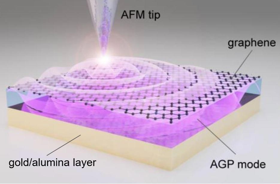
The first images of mid-infrared optical waves compressed 1,000 times captured using a highly sensitive scattering-type scanning near-field optical microscope.
KAIST researchers and their collaborators at home and abroad have successfully demonstrated a new methodology for direct near-field optical imaging of acoustic graphene plasmon fields. This strategy will provide a breakthrough for the practical applications of acoustic graphene plasmon platforms in next-generation, high-performance, graphene-based optoelectronic devices with enhanced light-matter interactions and lower propagation loss.
It was recently demonstrated that ‘graphene plasmons’ – collective oscillations of free electrons in graphene coupled to electromagnetic waves of light – can be used to trap and compress optical waves inside a very thin dielectric layer separating graphene from a metallic sheet. In such a configuration, graphene’s conduction electrons are “reflected” in the metal, so when the light waves “push” the electrons in graphene, their image charges in metal also start to oscillate. This new type of collective electronic oscillation mode is called ‘acoustic graphene plasmon (AGP)’.
The existence of AGP could previously be observed only via indirect methods such as far-field infrared spectroscopy and photocurrent mapping. This indirect observation was the price that researchers had to pay for the strong compression of optical waves inside nanometer-thin structures. It was believed that the intensity of electromagnetic fields outside the device was insufficient for direct near-field optical imaging of AGP.
Challenged by these limitations, three research groups combined their efforts to bring together a unique experimental technique using advanced nanofabrication methods. Their findings were published in Nature Communications.
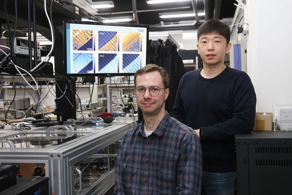
Direct Visualization Using Advanced Microscopy
A KAIST research team led by Professor Min Seok Jang from the School of Electrical Engineering used a highly sensitive scattering-type scanning near-field optical microscope (s-SNOM) to directly measure the optical fields of the AGP waves propagating in a nanometer-thin waveguide, visualizing thousand-fold compression of mid-infrared light for the first time.
Professor Jang and a post-doc researcher in his group, Sergey G. Menabde, successfully obtained direct images of AGP waves by taking advantage of their rapidly decaying yet always present electric field above graphene. They showed that AGPs are detectable even when most of their energy is flowing inside the dielectric below the graphene.
This became possible due to the ultra-smooth surfaces inside the nano-waveguides where plasmonic waves can propagate at longer distances. The AGP mode probed by the researchers was up to 2.3 times more confined and exhibited a 1.4 times higher figure of merit in terms of the normalized propagation length compared to the graphene surface plasmon under similar conditions.
Creating Ultra-Smooth Nano-Waveguides
These ultra-smooth nanostructures of the waveguides used in the experiment were created using a template-stripping method by Professor Sang-Hyun Oh and a post-doc researcher, In-Ho Lee, from the Department of Electrical and Computer Engineering at the University of Minnesota.
Professor Young Hee Lee and his researchers at the Center for Integrated Nanostructure Physics (CINAP) of the Institute of Basic Science (IBS) at Sungkyunkwan University synthesized the graphene with a monocrystalline structure, and this high-quality, large-area graphene enabled low-loss plasmonic propagation.
The chemical and physical properties of many important organic molecules can be detected and evaluated by their absorption signatures in the mid-infrared spectrum. However, conventional detection methods require a large number of molecules for successful detection, whereas the ultra-compressed AGP fields can provide strong light-matter interactions at the microscopic level, thus significantly improving the detection sensitivity down to a single molecule.
Applications in Optoelectronics and Sensing
Furthermore, the study conducted by Professor Jang and the team demonstrated that the mid-infrared AGPs are inherently less sensitive to losses in graphene due to their fields being mostly confined within the dielectric. The research team’s reported results suggest that AGPs could become a promising platform for electrically tunable graphene-based optoelectronic devices that typically suffer from higher absorption rates in graphene such as metasurfaces, optical switches, photovoltaics, and other optoelectronic applications operating at infrared frequencies.
Professor Jang said, “Our research revealed that the ultra-compressed electromagnetic fields of acoustic graphene plasmons can be directly accessed through near-field optical microscopy methods. I hope this realization will motivate other researchers to apply AGPs to various problems where strong light-matter interactions and lower propagation loss are needed.”
Reference: “Real-space imaging of acoustic plasmons in large-area graphene grown by chemical vapor deposition” by Sergey G. Menabde, In-Ho Lee, Sanghyub Lee, Heonhak Ha, Jacob T. Heiden, Daehan Yoo, Teun-Teun Kim, Tony Low, Young Hee Lee, Sang-Hyun Oh and Min Seok Jang, 19 February 2021, Nature Communications.
DOI: 10.1038/s41467-021-21193-5
This research was primarily funded by the Samsung Research Funding & Incubation Center of Samsung Electronics. The National Research Foundation of Korea (NRF), the U.S. National Science Foundation (NSF), Samsung Global Research Outreach (GRO) Program, and Institute for Basic Science of Korea (IBS) also supported the work.
Never miss a breakthrough: Join the SciTechDaily newsletter.
Follow us on Google and Google News.
1 Comment
This is the 2 hundredth “Breakthrough” this year alone. Who is buying up these patents and hiding them. I haven’t “Seen” a breakthrough in my 61 years. Still using gasoline. Still using radio signals. Still dying from cancer and other easily cured diseases.How about letting the small people have a breakthrough.