The emergence of artificial intelligence and machine learning techniques is changing the world dramatically with novel applications such as the Internet of Things, autonomous vehicles, real-time imaging processing, and big data analytics in healthcare. In 2020, the global data volume is estimated to reach 44 Zettabytes, and it will continue to grow beyond the current capacity of computing and storage devices. At the same time, the related electricity consumption will increase 15 times by 2030, swallowing 8% of the global energy demand. Therefore, reducing energy consumption and increasing the speed of information storage technology is in urgent need.
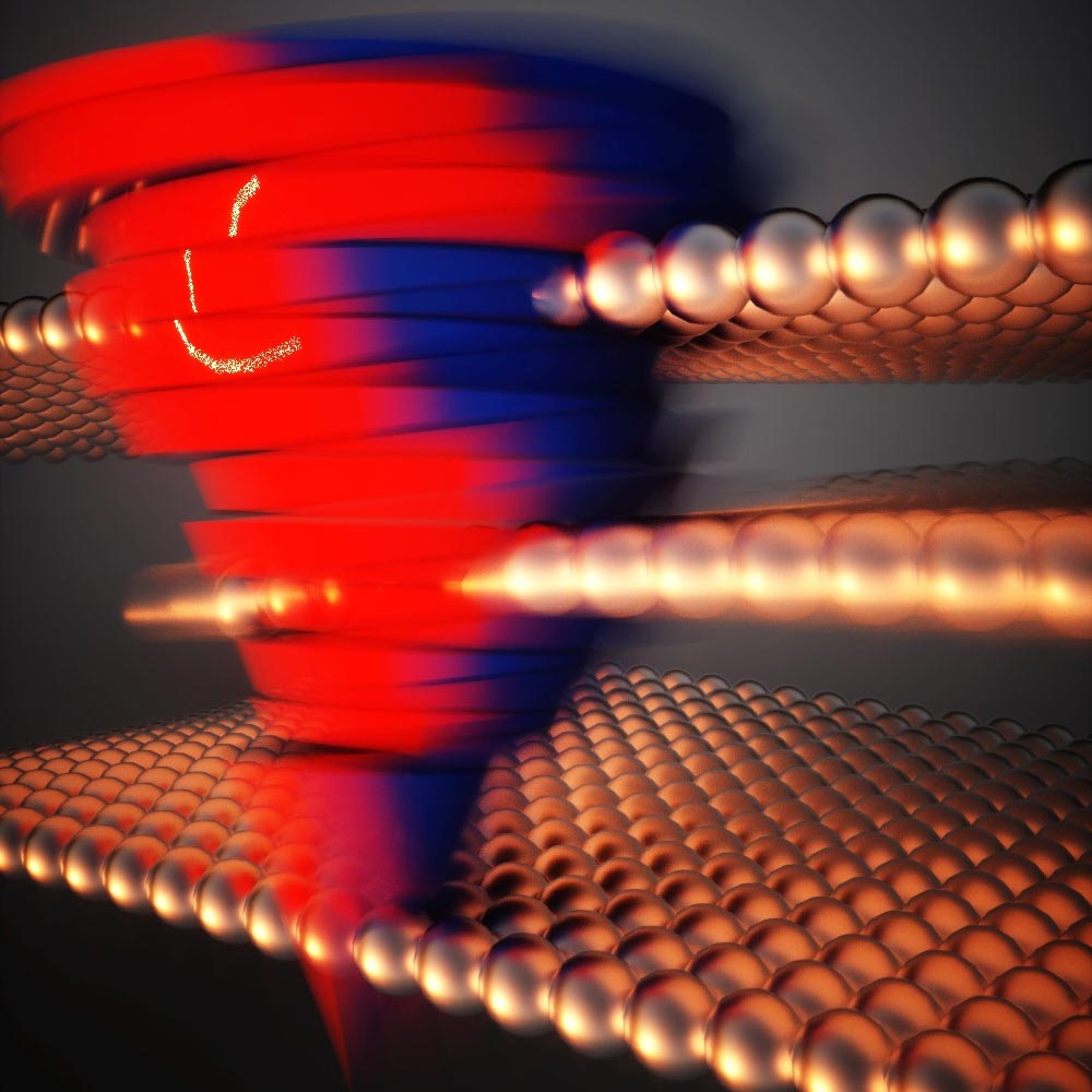
Berkeley researchers led by HKU President Professor Xiang Zhang when he was in Berkeley, in collaboration with Professor Aaron Lindenberg’s team at Stanford University, invented a new data storage method: They make odd-numbered layers slide relative to even-number layers in tungsten ditelluride, which is only 3nm thick. The arrangement of these atomic layers represents 0 and 1 for data storage. These researchers creatively make use of quantum geometry: Berry curvature, to read information out. Therefore, this material platform works ideally for memory, with independent ‘write’ and ‘read’ operation. The energy consumption using this novel data storage method can be over 100 times less than the traditional method.
This work is a conceptual innovation for non-volatile storage types and can potentially bring technological revolution. For the first time, the researchers prove that two-dimensional semi-metals, going beyond traditional silicon material, can be used for information storage and reading. This work was published in the latest issue of the journal Nature Physics.[1] Compared with the existing non-volatile (NVW) memory, this new material platform is expected to increase storage speed by two orders and decrease energy costs by three orders, and it can greatly facilitate the realization of emerging in-memory computing and neural network computing.
This research was inspired by the research of Professor Zhang’s team on “Structural phase transition of single-layer MoTe2 driven by electrostatic doping,”[2] published in Nature in 2017; and Lindenberg Lab’s research on “Use of light to control the switch of material properties in topological materials,” published in Nature in 2019.[3]
Previously, researchers found that in the two-dimensional material-tungsten ditelluride, when the material is in a topological state, the special arrangement of atoms in these layers can produce so-called “Weyl nodes,” which will exhibit unique electronic properties, such as zero resistance conduction. These points are considered to have wormhole-like characteristics, where electrons tunnel between opposite surfaces of the material. In previous experiment, the researchers found that the material structure can be adjusted by terahertz radiation pulse, thereby quickly switching between the topological and non-topological states of the material, effectively turning the zero-resistance state off and then on again. Zhang’s team has proved that the atomic-level thickness of two-dimensional materials greatly reduces the screening effect of the electric field, and its structure is easily affected by the electron concentration or electric field. Therefore, topological materials at two-dimensional limit can allow the turning of optical manipulation into electrical control, paving towards electronic devices.
In this work, the researchers stacked three atomic layers of tungsten ditelluride metal layers, like nanoscale deck of cards. By injecting a small amount of carriers into the stack or applying a vertical electric field, they caused each odd-numbered layer to slide laterally relative to the even-numbered layers above and below it. Through the corresponding optical and electrical characterizations, they observed that this slip is permanent until another electrical excitation triggers layers to rearrange. Furthermore, in order to read the data and information stored between these moving atomic layers, the researchers used the extremely large “Berry curvature” in the semi-metallic material. This quantum characteristic is like a magnetic field, which can steer electrons’ propagation and result in nonlinear Hall effect. Through such effect, the arrangement of the atomic layer can be read without disturbing the stacking.
Using this quantum characteristic, different stacks, and metal polarization states can be distinguished well. This discovery solves the long-term reading difficulty in ferroelectric metals due to their weak polarization. This makes ferroelectric metals not only interesting in basic physical exploration but also proves that such materials may have applicational prospects comparable to conventional semiconductors and ferroelectric insulators. Changing the stacking orders only involves the breaking of the Van der Waals bond. Therefore, the energy consumption is theoretically two orders of magnitude lower than the energy consumed by breaking covalent bond in traditional phase change materials and provides a new platform for the development of more energy-efficient storage devices and helps us move towards a sustainable and smart future.
References:
- “Berry curvature memory through electrically driven stacking transitions” by Jun Xiao, Ying Wang, Hua Wang, C. D. Pemmaraju, Siqi Wang, Philipp Muscher, Edbert J. Sie, Clara M. Nyby, Thomas P. Devereaux, Xiaofeng Qian, Xiang Zhang and Aaron M. Lindenberg, 29 June 2020, Nature Physics.
DOI: 10.1038/s41567-020-0947-0 - “Structural phase transition in monolayer MoTe2 driven by electrostatic doping” by Ying Wang, Jun Xiao, Hanyu Zhu, Yao Li, Yousif Alsaid, King Yan Fong, Yao Zhou, Siqi Wang, Wu Shi, Yuan Wang, Alex Zettl, Evan J. Reed and Xiang Zhang, 11 October 2017, Nature.
DOI: 10.1038/nature24043 - “An ultrafast symmetry switch in a Weyl semimetal” by Edbert J. Sie, Clara M. Nyby, C. D. Pemmaraju, Su Ji Park, Xiaozhe Shen, Jie Yang, Matthias C. Hoffmann, B. K. Ofori-Okai, Renkai Li, Alexander H. Reid, Stephen Weathersby, Ehren Mannebach, Nathan Finney, Daniel Rhodes, Daniel Chenet, Abhinandan Antony, Luis Balicas, James Hone, Thomas P. Devereaux, Tony F. Heinz, Xijie Wang and Aaron M. Lindenberg, 2 January 2019, Nature.
DOI: 10.1038/s41586-018-0809-4
Never miss a breakthrough: Join the SciTechDaily newsletter.
Follow us on Google and Google News.