New research boosts our understanding of a likely candidate for next-generation computer chips.
Scientists at the Princeton Plasma Physics Laboratory are advancing semiconductor technology by developing thinner, more efficient materials called transition-metal dichalcogenides (TMDs). These materials, only a few atoms thick, could lead to more compact and powerful computer chips. The research also investigates the role of defects within these materials, which can affect their electrical properties and potentially enhance their functionality.
The Evolution of Computer Chips
Silicon computer chips have served us well for more than half a century. The tiniest features on chips currently sold are approximately 3 nanometers — a startlingly small size given that a human hair is roughly 80,000 nanometers wide. Reducing the size of features on chips will help us meet our endless need for more memory and processing power in the palm of our hand. But the limit of what can be achieved with standard materials and processes is near.
Breakthroughs in Chip Materials
Researchers at the U.S. Department of Energy’s (DOE) Princeton Plasma Physics Laboratory (PPPL) are applying their expertise in physics, chemistry, and computer modeling to create the next generation of computer chips, aiming for processes and materials that will produce chips with smaller features.
“All of our existing electronic devices use chips made up of silicon, which is a three-dimensional material. Now, many companies are investing a lot in chips made up of two-dimensional materials,” said Shoaib Khalid, an associate research physicist at PPPL. The materials actually exist in three dimensions, but they are so thin — often made up of only a few layers of atoms — that scientists have taken to calling them 2D.
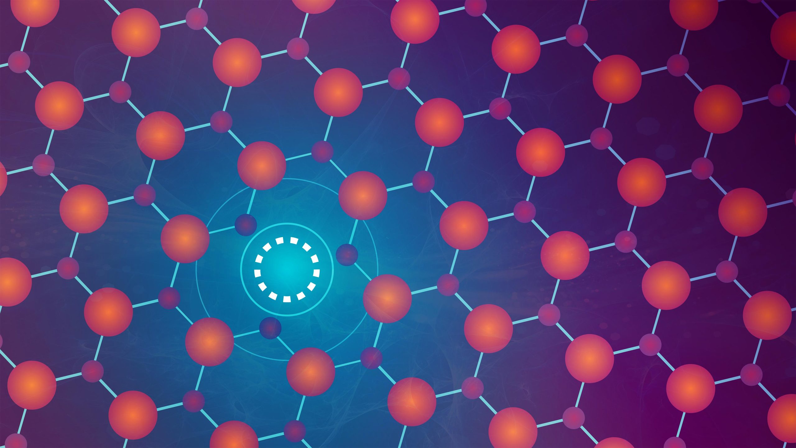
Two-dimensional (2D) materials are ultra-thin substances consisting of a single layer of atoms. These materials exhibit unique physical, chemical, and electronic properties distinct from their bulk counterparts, primarily due to their extreme thinness and high surface area. Graphene, a single layer of carbon atoms arranged in a hexagonal lattice, is the most well-known 2D material, celebrated for its strength, conductivity, and flexibility. Beyond graphene, other 2D materials include transition metal dichalcogenides (e.g., MoS₂), hexagonal boron nitride, and black phosphorus. These materials have potential applications in electronics, sensors, energy storage, and nanotechnology.
Transition-Metal Dichalcogenides: Next-Gen Semiconductors
Khalid, together with PPPL’s Bharat Medasani and Anderson Janotti from the University of Delaware, investigated one potential silicon replacement: a 2D material known as a transition-metal dichalcogenide (TMD).
Their new paper, published in the journal 2D Materials, details the variations that can occur in the atomic structure of TMDs, why they happen, and how they affect the material. Information about these variations lays the groundwork for refining the processes needed to create next-generation computer chips.
Ultimately, the goal is to design plasma-based manufacturing systems that can create TMD-based semiconductors made to the precise specifications required for the application.
TMD: A Tiny Metal Sandwich
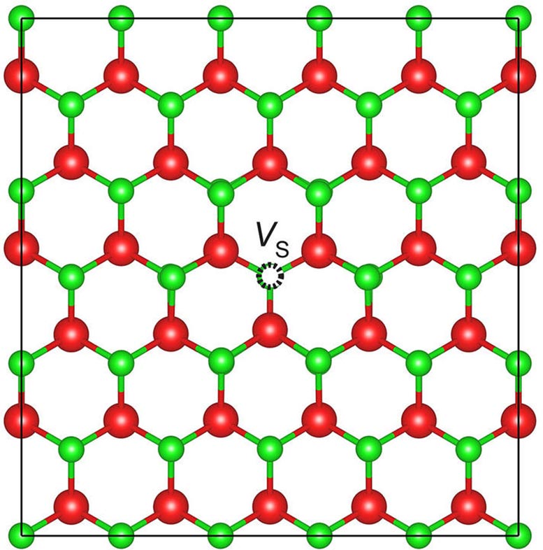
A TMD can be as thin as three atoms high. Think of it like a tiny metal sandwich. The bread is made of a chalcogen element: oxygen, sulfur, selenium or tellurium. The filling is a layer of transition metal — any metal from groups 3 to 12 in the periodic table of elements. A bulk TMD has five or more layers of atoms. The atoms are arranged in a crystal structure or lattice. Ideally, the atoms are organized in a precise and consistent pattern throughout the lattice. In reality, small alterations can be found in the pattern. One spot in the pattern might be missing an atom, or an atom might be found in an odd location. Scientists call these alterations defects, but they can have a beneficial impact on the material.
Some TMD defects, for example, can make the semiconductor more electrically conductive. Good or bad, it is critical that scientists understand why defects happen and how they will affect the material so they can incorporate or eliminate these defects as necessary. Understanding common defects also allows the researchers to explain the results from past experiments with TMDs.
“When bulk TMDs are made, they have excess electrons,” Khalid said, adding that researchers were not sure why these excess negatively charged particles were present. “In this work, we explain that the excess electrons can be caused by hydrogen.”
The researchers came to this conclusion after calculating the amount of energy that would be required to form different kinds of TMD defects. They looked at defects involving chalcogen vacancies, which were previously known to be present in TMDs, and defects involving hydrogen because this element is often present during the chip manufacturing process. Researchers are particularly interested in finding out which defects require minimal formation energy because these are the ones that are likely to occur — it doesn’t take much energy for them to happen!
The team then investigated the role of each of the low-formation-energy defects. Specifically, they wanted to know how each defect configuration might impact the electrical charge of the material. The researchers found that one of the defect configurations involving hydrogen provides excess electrons, which creates negatively charged semiconductor material, known as an n-type. Computer chips are made using combinations of n-type semiconductor material and positively charged, or p-type, material.
Research Insights on Chalcogen Vacancies
The other type of defect explored in the paper is known as a chalcogen vacancy: a missing atom of oxygen, sulfur, selenium or tellurium, depending on the type of TMD. The researchers focused on explaining the results of past experiments on flakes of the bulk TMD material molybdenum disulfide. The experiments, which involved shining light on the TMD, showed unexpected frequencies of light coming from the TMD. These unexpected frequencies, the researchers found, could be explained by the movement of electrons related to the chalcogen vacancy.
“This is a common defect. They can often see it from the images of scanning tunneling microscopes when they grow the TMD film,” Khalid said. “Our work provides a strategy to investigate the presence of these vacancies in the bulk TMDs. We explained past experimental results shown in molybdenum disulfide, and then we predicted a similar thing for other TMDs.”
The process suggested by the researchers involves analyzing the TMD for defects using measurement techniques called photoluminescence to see which frequencies of light are emitted by the material. The peak frequency of light can be used to determine the electron configurations of the atoms in the TMD and the presence of chalcogen defects. The journal article includes information about the frequencies that would be emitted by five types of TMDs with chalcogen vacancies, including molybdenum disulfide. The results, therefore, provide a guideline for investigating chalcogen vacancies in future experiments.
Reference: “Role of chalcogen vacancies and hydrogen in the optical and electrical properties of bulk transition-metal dichalcogenides” by Shoaib Khalid, Anderson Janotti and Bharat Medasani, 24 May 2024, 2D Materials.
DOI: 10.1088/2053-1583/ad4720
This work was supported by the DOE under grant DE-AC02-09CH11466 and the National Science Foundation (NSF) award #OIA-2217786. Calculations were carried out at the National Energy Research Scientific Computing Center (NESRC) under contract number DE-AC02-05CH11231 using NERSC award BES-ERCAP27253, the Stellar cluster at Princeton University and the DARWIN computing system at the University of Delaware, using the NSF grant 1919839.
Never miss a breakthrough: Join the SciTechDaily newsletter.
Follow us on Google and Google News.