Researchers at the University of Konstanz have successfully filmed the operations of extremely fast electronic circuitry in an electron microscope at a bandwidth of tens of terahertz.
The increasing demand for ever-faster information processing has ushered in a new era of research focused on high-speed electronics operating at frequencies nearing terahertz and petahertz regimes. While existing electronic devices predominantly function in the gigahertz range, the forefront of electronics is pushing towards millimeter waves, and the first prototypes of high-speed transistors, hybrid photonic platforms, and terahertz metadevices are starting to bridge the electronic and optical domains.
However, characterizing and diagnosing such devices pose a significant challenge due to the limitations of available diagnostic tools, particularly in terms of speed and spatial resolution. How shall one measure a breakthrough device if it’s the fastest and smallest of its kind?
Innovative Diagnostic Solution
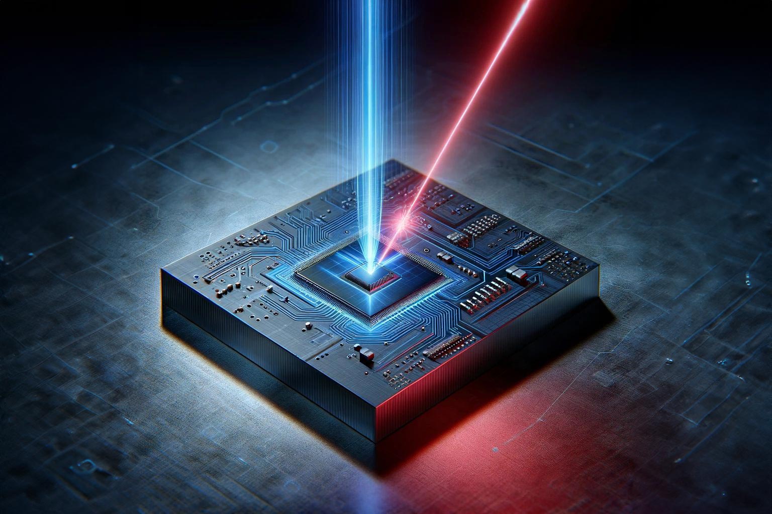
In response to this challenge, a team of researchers from the University of Konstanz now proposes an innovative solution: They create femtosecond electron pulses in a transmission electron microscope, compress them with infrared laser light to merely 80 femtosecond duration, and synchronize them to the inner fields of a laser-triggered electronic transmission line with the help of a photoconductive switch. Then, using a pump-probe approach, the researchers directly sense the local electromagnetic fields in their electronic devices as a function of space and time.
This new kind of ultrafast electron beam probe provides femtosecond, nanometer, and millivolt resolutions under normal operating conditions, that is, without affecting the in-situ operation of the device. Only the substrate material needs to be thinned out to become transparent to the electron beam.
Advancing Next-Generation Electronics
This femtosecond electron beam probe approach opens up new frontiers in the research and development of next-generation electronics because diagnostic resolutions are now, in principle, only limited by the de Broglie wavelength of the electrons in the microscope and the cycle period of the infrared laser light that is applied for the all-optical electron pulse compression.
With such resolutions, the new tool offers unprecedented insight into future electronic circuitry and can guide their design towards novel applications.
The new concept’s versatility and seamless integration into existing electron-beam inspection devices in the semiconductor industry should make it a promising asset for advancing ultrafast electronics toward unexplored capacities.
Reference: “Femtosecond electron beam probe of ultrafast electronics” by Maximilian Mattes, Mikhail Volkov and Peter Baum, 26 February 2024, Nature Communications.
DOI: 10.1038/s41467-024-45744-8
Funding: German Research Foundation (DFG) in the context of the Collaborative Research Centre “Fluctuations and Nonlinearities in Classical and Quantum Matter beyond Equilibrium” (SFB 1432); Marie Skłodowska-Curie grant no. 896148-STMICRO; University of Konstanz’s Young Scholar Fund.
Never miss a breakthrough: Join the SciTechDaily newsletter.
Follow us on Google and Google News.