Close Menu
    Facebook X (Twitter) Instagram
    SciTechDaily
    • Biology
    • Chemistry
    • Earth
    • Health
    • Physics
    • Science
    • Space
    • Technology
    Facebook X (Twitter) Pinterest YouTube RSS
    SciTechDaily
    Home»Technology»Enabling Better Optoelectronic Devices With Thin Cuprous Iodide Film
    Technology

    Enabling Better Optoelectronic Devices With Thin Cuprous Iodide Film

    By RIKENApril 17, 2021No Comments3 Mins Read
    Facebook Twitter Pinterest Telegram LinkedIn WhatsApp Email Reddit
    Share
    Facebook Twitter LinkedIn Pinterest Telegram Email Reddit
    Cuprous Iodide Crystals on Indium Arsenide Substrate
    Figure 1: A thin film of cuprous iodide crystals (blue) on an indium arsenide substrate (yellow). The sample’s purity was tested by shining photons onto the surface to create electron–hole pairs (red and blue spheres) and monitoring the light that was emitted (white rays). Credit: © 2021 RIKEN Center for Emergent Matter Science

    Better optoelectronic devices could be realized using a high-quality film of cuprous iodide.

    A defect-free thin film of cuprous iodide—made up of just one crystal—has been fabricated by RIKEN physicists1. The atomically flat sample is a boost for producing better semiconductors.

    Semiconductors lie at the heart of many optoelectronic devices including lasers and light-emitting diodes (LEDs). Engineers would love to use cuprous iodide—an example of a halide compound—for semiconductors because it is an excellent conductor that is stable above room temperature. The trouble is that it is tough to fabricate a genuinely thin film of cuprous iodide without impurities. The usual method involves depositing the film from a solution. “But a solution process can’t make a high-quality thin film from cuprous iodide,” says Masao Nakamura of the RIKEN Center for Emergent Matter Science.

    Instead, Nakamura and his co-workers used an alternative technique known as molecular beam epitaxy, in which the film is gradually grown on top of a substrate, at an elevated temperature, and in a vacuum. Molecular beam epitaxy is already commonly employed in manufacturing semiconductors. But it is hard to use for cuprous iodide because the material is highly volatile—meaning that it easily evaporates during the process, rather than settling into a film. To overcome this difficulty, the team began growing their film at a lower temperature and then increased the temperature. “This two-step process we newly developed was highly effective,” says Nakamura.

    The Role of Indium Arsenide Substrates

    The team had another trick to raise the quality of their film. They chose indium arsenide as the substrate since its lattice spacing is very similar to that of cuprous iodide. “If the lattice spacing is not well matched, many defects will form in the material,” explains Nakamura.

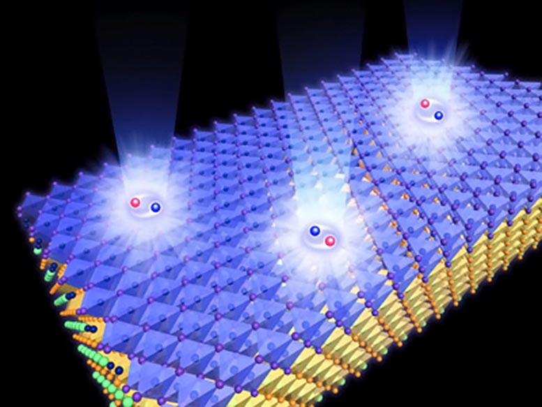
    Nakamura and his colleagues then tested the purity of their sample using a technique called photoluminescence spectroscopy, which involves firing photons, or particles of light, at the surface of the material. These photons are absorbed by the material, exciting its electrons to a higher energy state and causing them to emit new photons (Fig. 1). Monitoring the emitted light allowed the team to determine that they had created a single-crystal film, free from defects. “We expected the quality to improve using our method,” says Nakamura. “But the results exceeded our expectations.”

    Nakamura and his team now plan to sandwich together semiconductors made of different halides and investigate new properties that arise. “We will explore emerging novel functionalities and physics at the halide interfaces,” says Nakamura.

    Reference: “Heteroepitaxial growth of wide bandgap cuprous iodide films exhibiting clear free-exciton emission” by S. Inagaki, M. Nakamura, Y. Okamura, M. Ogino, Y. Takahashi, L. C. Peng, X. Z. Yu, Y. Tokura and M. Kawasaki, 5 January 2021, Applied Physics Letters.
    DOI: 10.1063/5.0036862

    Never miss a breakthrough: Join the SciTechDaily newsletter.
    Follow us on Google and Google News.

    Materials Science Optics RIKEN
    Share. Facebook Twitter Pinterest LinkedIn Email Reddit

    Related Articles

    Tiny Three-Dimensional Chessboards Could Lead to “Paper Electronics”

    Breakthrough Could Lead to Cameras That Can Capture Images Using Ambient Radio Waves

    High-Performance Laser Fabrication Breakthrough Promises Low Cost Lasers

    Researchers Create ‘Intelligent’ Interaction Between Light and Material – New Form of Computing

    “Perfect” Solar Energy Absorber Created by Laser Etching Metal With Nanoscale Structures

    New Wavelength Detector Could Improve Data Communications

    New Material Can Be Molded into Highly Conductive 3D Structures

    Thermal Cloak Molds the Flow of Heat Around an Object

    Researchers Reveal the Cause of LED Efficiency Droop

    Leave A Reply Cancel Reply

    • Facebook
    • Twitter
    • Pinterest
    • YouTube

    Don't Miss a Discovery

    Subscribe for the Latest in Science & Tech!

    Trending News

    Mezcal “Worm” in a Bottle Mystery: DNA Testing Reveals a Surprise

    New Research Reveals That Your Morning Coffee Activates an Ancient Longevity Switch

    This Is What Makes You Irresistible to Mosquitoes

    Shockingly Powerful Giant Octopuses Ruled the Seas 100 Million Years Ago

    Scientists Stunned by New Organic Molecules Found on Mars

    Rewriting Dinosaur Evolution: Scientists Unearth Remarkable 150-Million-Year-Old Stegosaur Skull

    Omega-3 Supplements Linked to Cognitive Decline in Surprising New Study

    First-of-Its-Kind Discovery: Homer’s Iliad Found Embedded in a 1,600-Year-Old Egyptian Mummy

    Follow SciTechDaily
    • Facebook
    • Twitter
    • YouTube
    • Pinterest
    • Newsletter
    • RSS
    SciTech News
    • Biology News
    • Chemistry News
    • Earth News
    • Health News
    • Physics News
    • Science News
    • Space News
    • Technology News
    Recent Posts
    • New Research Challenges Long-Held Beliefs About How the Brain Makes Decisions
    • Breakthrough Technology Reveals New Treatment Targets for Cancer
    • Scientists Discover New Way To Make Drug-Resistant Cancer Treatable Again
    • This Simple Exercise Trick Builds Muscle With Less Effort, Study Finds
    • Middle Age Is Becoming a Breaking Point in America, Study Reveals
    Copyright © 1998 - 2026 SciTechDaily. All Rights Reserved.
    • Science News
    • About
    • Contact
    • Editorial Board
    • Privacy Policy
    • Terms of Use

    Type above and press Enter to search. Press Esc to cancel.