Scientists at the Oak Ridge National Laboratory studied hafnia’s potential in semiconductor applications, revealing its behavior can be influenced by the surrounding atmosphere. Their findings offer promising implications for future memory technologies.
A team of scientists from the Department of Energy’s Oak Ridge National Laboratory has investigated the behavior of hafnium oxide, or hafnia, because of its potential for use in novel semiconductor applications.
Materials like hafnia display ferroelectricity, meaning they can store data for extended periods even without power. Such characteristics suggest these materials could be pivotal in developing new nonvolatile memory technologies. Innovative nonvolatile memory applications will pave the way for the creation of bigger and faster computer systems by alleviating the heat generated from the continual transfer of data to short-term memory.
Understanding Hafnia’s Electrical Behavior
The scientists explored whether the atmosphere plays a role in hafnia’s ability to change its internal electric charge arrangement when an external electric field is applied. The goal was to explain the range of unusual phenomena that have been obtained in hafnia research. The team’s findings were recently published in the journal Nature Materials.
“We have conclusively proven that the ferroelectric behavior in these systems is coupled to the surface and is tunable by changing the surrounding atmosphere. Previously, the workings of these systems were speculation, a hypothesis based on a large number of observations both by our group and by multiple groups worldwide,” said ORNL’s Kyle Kelley, a researcher with the Center for Nanophase Materials Sciences. CNMS is a DOE Office of Science user facility.
Kelley performed the experiments and envisioned the project in collaboration with Sergei Kalinin of the University of Tennessee, Knoxville.
Surface Layer and Memory Application
Materials typically used in memory applications have a surface, or dead, layer that interferes with the material’s ability to store information. As materials are scaled down to only several nanometers thick, the effect of the dead layer becomes extreme enough to completely stop the functional properties. By changing the atmosphere, the scientists were able to tune the surface layer’s behavior, which, in hafnia, transitioned the material from the antiferroelectric to the ferroelectric state.
“Ultimately, these findings provide a pathway for predictive modeling and device engineering of hafnia, which is urgently needed, given the importance of this material in the semiconductor industry,” Kelley said.
Predictive modeling enables scientists to use previous research to estimate the properties and behavior of an unknown system. The study that Kelley and Kalinin led focused on hafnia alloyed, or blended, with zirconia, a ceramic material. However, future research could apply the findings to anticipate how hafnia may behave when alloyed with other elements.
Research Methods and Collaboration
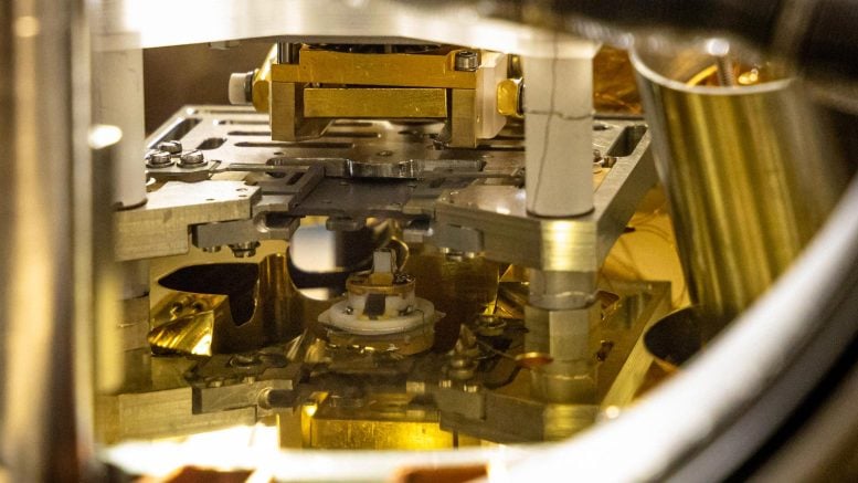
The research relied on atomic force microscopy both inside a glovebox and in ambient conditions, as well as ultrahigh-vacuum atomic force microscopy, methods available at the CNMS.
“Leveraging the unique CNMS capabilities enabled us to do this type of work,” Kelley said. “We basically changed the environment all the way from ambient atmosphere to ultrahigh vacuum. In other words, we removed all gases in the atmosphere to negligible levels and measured these responses, which is extremely hard to do.”
Team members from the Materials Characterization Facility at Carnegie Mellon University played a key role in the research by providing electron microscopy characterization, and collaborators from the University of Virginia led the materials development and optimization.
ORNL’s Yongtao Liu, a researcher with CNMS, performed ambient piezoresponse force microscopy measurements.
The model theory that underpinned this research project was the result of a long research partnership between Kalinin and Anna Morozovska at the Institute of Physics, National Academy of Sciences of Ukraine.
Insights from the Team
“I have worked with my colleagues in Kyiv on physics and chemistry of ferroelectrics for almost 20 years now,” Kalinin said. “They did a lot for this paper while almost on the front line of the war in that country. These people keep doing science in conditions that most of us cannot imagine.”
The team hopes that what they have discovered will stimulate new research specific to exploring the role of controlled surface and interface electrochemistries — the relationship between electricity and chemical reactions — in a computing device’s performance.
“Future studies can extend this knowledge to other systems to help us understand how the interface affects the device properties, which, hopefully, will be in a good way,” Kelley said. “Typically, the interface kills your ferroelectric properties when scaled to these thicknesses. In this case, it showed us a transition from one material state to another.”
Kalinin added: “Traditionally, we explored surfaces at the atomic level to understand phenomena such as chemical reactivity and catalysis, or the modification of the rate of a chemical reaction. Simultaneously, in traditional semiconductor technology, our goal was only to keep surfaces clean from contaminants. Our studies show that, in fact, these two areas — the surface and the electrochemistry — are connected. We can use surfaces of these materials to tune their bulk functional properties.”
The title of the paper is “Ferroelectricity in hafnia controlled via surface electrochemical state.”
Reference: “Ferroelectricity in hafnia controlled via surface electrochemical state” by Kyle P. Kelley, Anna N. Morozovska, Eugene A. Eliseev, Yongtao Liu, Shelby S. Fields, Samantha T. Jaszewski, Takanori Mimura, Sebastian Calderon, Elizabeth C. Dickey, Jon F. Ihlefeld and Sergei V. Kalinin, 14 August 2023, Nature Materials.
DOI: 10.1038/s41563-023-01619-9
This research was supported as part of the Center for 3D Ferroelectric Microelectronics, an Energy Frontier Research Center funded by DOE’s Office of Science, Basic Energy Sciences program, and was partially performed as a user proposal at the CNMS.
Never miss a breakthrough: Join the SciTechDaily newsletter.
Follow us on Google and Google News.